Switch Control
_HIGH_VOLTAGE_AC_SWITCHER
Published:2009/7/8 22:16:00 Author:May | From:SeekIC
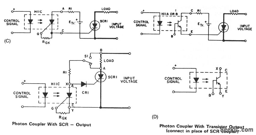
In Fig. 67-1C, R1 can be connected to Point A, which will remove the voltage from the coupler after SCR1 is triggered, or to Point B so that the coupler output will always be biased by input voltage. The former is preferred since it decreases the power dissipation in R1. A more practical form of SCR triggering is shown in Fig. 67-1F. Trigger energy is obtained from the anode supply and stored in C1. Coupler voltage is limited by the zener voltage. This approach permits switching of higher voltages than the blocking voltage capability of the output device of the photon coupler. To reduce the power losses in R1 and to obtain shorter time constants for charging C1, the zener diode is used instead of a resistor.
Reprinted Url Of This Article:
http://www.seekic.com/circuit_diagram/Control_Circuit/Switch_Control/_HIGH_VOLTAGE_AC_SWITCHER.html
Print this Page | Comments | Reading(3)

Article Categories
power supply circuit
Amplifier Circuit
Basic Circuit
LED and Light Circuit
Sensor Circuit
Signal Processing
Electrical Equipment Circuit
Control Circuit
Remote Control Circuit
A/D-D/A Converter Circuit
Audio Circuit
Measuring and Test Circuit
Communication Circuit
Computer-Related Circuit
555 Circuit
Automotive Circuit
Repairing Circuit
Code: