power supply circuit
Dual Output Power Supply +/-53V / 3A based on Transistors
Published:2013/3/18 21:21:00 Author:Ecco | Keyword: Dual Output Power Supply, +/-53V / 3A, Transistors | From:SeekIC
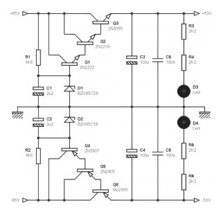
This is the circuit diagram of dual output power supply +/-53V / 3A based on transistors. This circuit has been designed for audio amplifier power supply requires a symmetrical + / -53 V (+ / -56 V maximum). The role of the circuit part presented here is to lower the voltage of both positive and negative lines of + / -65 V for non-hazardous + / -53 V for the amplifier, while allowing the current to 3 A in continuous operation.
The diagram above, based on the same principle as the previous circuit Dual supply + /-15V-based transistors, and is based on the use of common components. Differences of Dual supply + /-15V-based transistors, lies only in the number of transistors connected in cascade to allow high output currents while not requiring a zener diode of 10 W for output voltage stabilization. The main advantage of this type of configuration is to have a high current gain. The second point is not important in this case. Power dissipation in the ‘final’ two transistor Q3, and Q6 to 3 A output current, is about 36 W, which require a large heatsink. Transistors Q2 and Q5 is recommended fitted fin heat sink (for TO5 case).
Reprinted Url Of This Article:
http://www.seekic.com/circuit_diagram/Power_Supply_Circuit/Dual_Output_Power_Supply____53V___3A_based_on_Transistors.html
Print this Page | Comments | Reading(3)

Article Categories
power supply circuit
Amplifier Circuit
Basic Circuit
LED and Light Circuit
Sensor Circuit
Signal Processing
Electrical Equipment Circuit
Control Circuit
Remote Control Circuit
A/D-D/A Converter Circuit
Audio Circuit
Measuring and Test Circuit
Communication Circuit
Computer-Related Circuit
555 Circuit
Automotive Circuit
Repairing Circuit
Code: