Switching-Regulator Circuit
Regulated power supply circuit diagram used VMOS as switching element
Published:2011/4/8 2:38:00 Author:Nicole | Keyword: regulated power supply, switching element | From:SeekIC
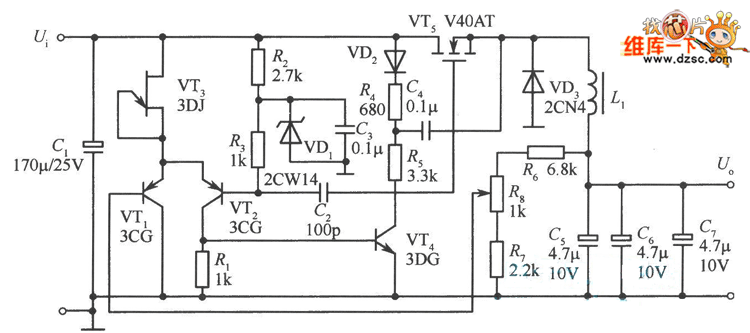
As shown, it is a power supply circuit used VMOS as switching element. VT5 is VMOS power transistor, the switch adjustment element of power supply; L1is the energy storage inductor; VD3 for the freewheeling diode; VT3 for the FET, as the constant current source of VTl, VT2, to provide the emitter with lmA constant current; Cl is the input filter capacitor; C5, C6, C7 is the output filter capacitor.
It is determined by the relative voltage of the two base to turn on VTl or VT2 first. If the base potential of VT1 below VT2, the VTl on, VT2 off; on the contrary, the VTl off, VT2 on. The base potential of VT2 is decided by resistances R2, R3 and voltage regulator diode VD1, it is a constant; and base potential of VTl is obtained from the output voltage through the resistor R6C R, and derived from the potentiometer R8, the output voltage can be changed by adjusting potentiometer R8.
In order to reduce the power consumption of switch regulator VT5, to improve its turning speed, the circuit adopts bootstrap network which composed of R5, C4. When VT5 is off, the source potential is 0V, the input voltage charge to C4 through diode VD2 resistor R4, so that the voltage on C4 is close to the input voltage. When VT5 is on, the source potential rise, as there is sufficient voltage on the capacitor C4, so that the diode VD2 off, by this time, the voltage on R5 is close to 2 times the input voltage, so VT5 turn on more quickly. At this point even if the input voltage is low, the circuit also can be flipped. The role of C2, C3 is to make VT1, VT2 flip quickly, then to improve the speed of switching.
Reprinted Url Of This Article:
http://www.seekic.com/circuit_diagram/Power_Supply_Circuit/Switching-Regulator_Circuit/Regulated_power_supply_circuit_diagram_used_VMOS_as_switching_element.html
Print this Page | Comments | Reading(3)

Article Categories
power supply circuit
Amplifier Circuit
Basic Circuit
LED and Light Circuit
Sensor Circuit
Signal Processing
Electrical Equipment Circuit
Control Circuit
Remote Control Circuit
A/D-D/A Converter Circuit
Audio Circuit
Measuring and Test Circuit
Communication Circuit
Computer-Related Circuit
555 Circuit
Automotive Circuit
Repairing Circuit
Code: