Switching-Regulator Circuit
Single-ended flyback switching power supply circuit diagram of capacitance-type pressure clamp
Published:2011/3/22 21:48:00 Author:Nicole | Keyword: switching power supply | From:SeekIC
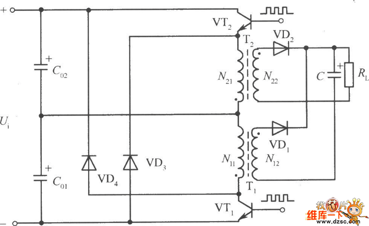
As shown, when the VT1 turns on, charging capacitor C02, C01 discharging, the primary winding N11 of the transformer Tl is applied to about l / 2 of the input voltage; when VTl stops, the voltage of N11 is polarity reversal, the emitter voltage Uce1 of VT1 reach the input voltage Ui, the diode VD4 turns on, Ucel is clamped; Similarly, VT2 turns on, C02 discharging, C01 charging, the primary winding N21 of T2 is applied to about 1 / 2 of the input voltage; VT2 stops, the voltage of N21 is polarity reversal, after VD3 turns on , Uce2 is also clamped to the input voltage Ui.
Reprinted Url Of This Article:
http://www.seekic.com/circuit_diagram/Power_Supply_Circuit/Switching-Regulator_Circuit/Single_ended_flyback_switching_power_supply_circuit_diagram_of_capacitance_type_pressure_clamp.html
Print this Page | Comments | Reading(3)

Article Categories
power supply circuit
Amplifier Circuit
Basic Circuit
LED and Light Circuit
Sensor Circuit
Signal Processing
Electrical Equipment Circuit
Control Circuit
Remote Control Circuit
A/D-D/A Converter Circuit
Audio Circuit
Measuring and Test Circuit
Communication Circuit
Computer-Related Circuit
555 Circuit
Automotive Circuit
Repairing Circuit
Code: