Signal Processing
555 gradually ringing type sleep wake-up device circuit
Published:2011/5/24 22:56:00 Author:TaoXi | Keyword: gradually, ringing, sleep, wake-up | From:SeekIC
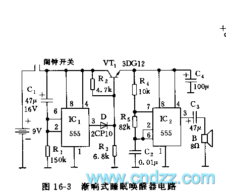
As the figure 16-3 shows, the delay switch circuit is composed of the IC1 and the R1,C1, the 800Hz multivibrator is composed of the IC2 and R4,R5,C2. When the electric clock's timing contact points turn on the power supply of this circuit,and thecapacitor C1's voltage can not be mutated, so pin-2 of 555 has the high electrical level. At this time, the 555's output port has the low electrical level, the diode D cuts off. When the electric potential of IC1's pin-2 and pin-6 drops to 1/3VDD, the circuit reverses, and the pin-3 has the high electrical level, this charging delay time is about 8 seconds. Then D conducts, the b electrode's potential of the VT1 tube increases.
Reprinted Url Of This Article:
http://www.seekic.com/circuit_diagram/Signal_Processing/555_gradually_ringing_type_sleep_wake_up_device_circuit.html
Print this Page | Comments | Reading(3)

Article Categories
power supply circuit
Amplifier Circuit
Basic Circuit
LED and Light Circuit
Sensor Circuit
Signal Processing
Electrical Equipment Circuit
Control Circuit
Remote Control Circuit
A/D-D/A Converter Circuit
Audio Circuit
Measuring and Test Circuit
Communication Circuit
Computer-Related Circuit
555 Circuit
Automotive Circuit
Repairing Circuit
Code: