Series: -
Transistor Type: NPN
Resistor - Base (R1) (Ohms): -
Current - Collector Cutoff (Max): -
Resistor - Emitter Base (R2) (Ohms): -
Frequency - Transition: -
Mounting Type: Through Hole
Current - Collector (Ic) (Max): 5A
Packaging: Tube
Power - Max: 100W
Vce Saturation (Max) @ Ib, Ic: 1V @ 400mA, 2A
Manufacturer: Toshiba
Voltage - Collector Emitter Breakdown (Max): 800V
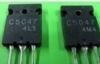
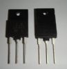
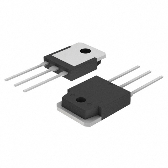
Package / Case: TO-3P-3, SC-65-3
DC Current Gain (hFE) (Min) @ Ic, Vce: 10 @ 1mA, 5V
Supplier Device Package: TO-3P(N)
DescriptionThe 2SC5354 is designed as toshiba transistor silicon NPN epitaxial planar type for high speed and high voltage switching applications and switching regulator applications and high speed DC-DC converter applications.
2SC5354 has two features. (1)Excellent switching times which would be max 0.7us for tT and would be max 0.5us for tf. (2)High collector breakdown voltage which would be 800V. Those are all the main features.
Some absolute maximum ratings of 2SC5354 have been concluded into several points as follow. (1)Its collector to base voltage would be 900V. (2)Its collector to emitter voltage would be 800V. (3)Its emitter to base voltage would be 7V. (4)Its collector current would be 5A for DC and would be 10A for pulse. (5)Its base current would be 2A. (6)Its collector power dissipation would be 100W. (7)Its junction temperature would be 150°C. (8)Its storage temperature range would be from -55°C to 150°C. It should be noted that stresses above those listed in absolute maximum ratings may cause permanent damage to device.
Also some electrical characteristics of 2SC5354 are concluded as follow. (1)Its collector cutoff current would be max 100uA with conditions of Vcb=800V and Ie=0. (2)Its emitter cutoff current would be max 1mA with conditions of Veb=7V and Ic=0. (3)Its DC current gain would be min 10 with conditions of Vce=5V and Ic=10mA. (4)Its collector to emitter saturation voltage would be max 1.0V with conditions of Ic=2A and Ib=0.4A. (5)Its base to emitter voltage would be max 1.3V with conditions of Ic=2A and Ib=0.4A. (6)Its collector to base breakdown voltage would be min 900V. (7)Its collector to emitter breakdown voltage would be min 800V.
It should be noted that the information about 2SC5354 contained herein is presented only as a guide for the applications of toshiba products. No responsibility is assumed by toshiba sorporation for any infringements of implication or otherwise under any intellectual property or other rights of toshiba corporation or others. And so on. If you have any question or suggestion or want to know more information please contact us for details. Thank you!
Parameters: | Technical/Catalog Information | 2SC5354 |
| Vendor | Toshiba |
| Category | Discrete Semiconductor Products |
| Transistor Type | NPN |
| Voltage - Collector Emitter Breakdown (Max) | 800V |
| Current - Collector (Ic) (Max) | 5A |
| Power - Max | 100W |
| DC Current Gain (hFE) (Min) @ Ic, Vce | 10 @ 10mA, 5V |
| Vce Saturation (Max) @ Ib, Ic | 1V @ 400mA, 2A |
| Frequency - Transition | - |
| Current - Collector Cutoff (Max) | - |
| Mounting Type | Through Hole |
| Package / Case | 2-16C1A (TO-247 N) |
| Packaging | Tube |
| Drawing Number | * |
| Lead Free Status | Contains Lead |
| RoHS Status | RoHS Non-Compliant |
| Other Names | 2SC5354
2SC5354
|
 2SC5354 Data Sheet