33291L

Features: • Designed to Operate Over Wide Supply Voltages of 5.5 to 26.5 V• Interfaces to Microprocessor Using 8-Bit SPI I/O Protocol up to 3.0 MHz• 1.0 A Peak Current Outputs with Maximum R DS(on) of 1.6 Ω at TJ - 150°C• Outputs Current Limited to Accommodate In-rush...

product image

33291L Picture
SeekIC No. : 004228383 Detail

33291L: Features: • Designed to Operate Over Wide Supply Voltages of 5.5 to 26.5 V• Interfaces to Microprocessor Using 8-Bit SPI I/O Protocol up to 3.0 MHz• 1.0 A Peak Current Outputs with...

floor Price/Ceiling Price

Part Number:
33291L
Supply Ability:
5000

Price Break

  • Qty
  • 1~5000
  • Unit Price
  • Negotiable
  • Processing time
  • 15 Days
Total Cost: $ 0.00

SeekIC Buyer Protection PLUS - newly updated for 2013!

  • Escrow Protection.
  • Guaranteed refunds.
  • Secure payments.
  • Learn more >>

Month Sales

268 Transactions

Rating

evaluate  (4.8 stars)

Upload time: 2024/4/18

Payment Methods

All payment methods are secure and covered by SeekIC Buyer Protection PLUS.

Notice: When you place an order, your payment is made to SeekIC and not to your seller. SeekIC only pays the seller after confirming you have received your order. We will also never share your payment details with your seller.
Product Details

Description


Features:

• Designed to Operate Over Wide Supply Voltages of 5.5 to 26.5 V
• Interfaces to Microprocessor Using 8-Bit SPI I/O Protocol up to 3.0 MHz
• 1.0 A Peak Current Outputs with Maximum R DS(on) of 1.6 Ω at TJ - 150°C
• Outputs Current Limited to Accommodate In-rush Currents Associated with Switching Incandescent Loads
• Output Voltages Clamped to 53 V During Inductive Switching
• Maximum Sleep Current (IPWR) of 25 µA
• Maximum of 4.0 mA IDD During Operation


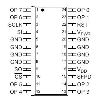
Pinout

  Connection Diagram


Specifications

Ratings Symbol
Value
Unit
Power Supply Voltage
Normal Operation (Steady-State)
Transient Conditions (Note 1)
V PWR(SUS)
V PWR(PK)
- 1.5 to 26.5
- 13 to 60
V
Logic Supply Voltage (Note 2)
VDD
- 0.3 to 7.0
V
Input Pin Voltage (Note 3)
VIN
- 0.3 to 7.0
V
Output Clamp Voltage (Note 4)
5.0 mA Iout 0.5 A
V OUT(OFF)
45 to 65
V
Output Self-Limit Current
I OUT(LIM)
1.0 to 3.0
A
Continuous Per Output Current (Note 5)
I OUT(CONT)
500
MA
ESD Voltage (Note 6)
Human Body Model (Note 7)
Machine Model (Note 8)
VESD1
VESD2
2000
200
V
Output Clamp Energy (Note 9)
ECLAMP
50
MHz
Recommended Frequency of SPI Operation

fSPI
3.0
°C
Storage Temperature
TSTG
- 55 to 150
°C
Operating Case Temperature
TC
- 40 TO 125
°C
Operating Junction Temperature
TJ
- 40 TO 150
Power Dissipation (TA = 25° C) (Note 10)
PD
2.0
°C
Soldering Temperature (Note 11)
TSOLDER
260
W
Thermal Resistance (Junction-to-Ambient)
Case 751E-04 Package
All Outputs ON (Note 12)
Single Output ON (Note 13)
RJA
45
60
°C/W
Notes:
1. Transient capability with external 100 Ω resistor in series with VP pin and supply.
2. Exceeding these limits may cause a malfunction or permanent damage to the device.
3. Exceeding the limits on SCLK, SI, CS, SFPD, or RST pins may cause permanent damage to the device.
4. With output OFF.
5. Continuous output current rating so long as maximum junction temperature is not exceeded. Operation at 125°C ambient temperature will
require maximum output current computation using package RJA.
6. ESD data available upon request.
7. ESD1 testing is performed in accordance with the Human Body Model (CZap = 200 pF, RZap = 1500 Ω).
8. ESD2 testing is performed in accordance with the Machine Model (CZap = 200pF, RZap = 0 Ω).
9. Maximum output clamp energy capability at 150°C junction temperature using a single non-repetitive pulse method.
10. Maximum power dissipation at indicated junction temperature with no heat sink used.
11. Lead soldering temperature limit is for 10 seconds maximum duration; not designed for immersion soldering; exceeding these limits may
cause malfunction or permanent damage to the device.Contact Motorola Sales Office for device immersion soldering time/temperature limits.
12. Thermal resistance from Junction-to-Ambient with all outputs ON and dissipating equal power.
13. Thermal resistance from Junction -to-Ambient with a single output ON.


Description

The 33291L device is an eight output, low side power switch with 8-bit serial input control. The 33291L is a versatile circuit designed for automotive applications, but is well suited for other environments. The 33291L incorporates SMAROSTM technology, with CMOS logic, bipolar/MOS analog circuitry, and DMOS power MOSFETs. The 33291L interfaces directly with a microcontroller to control various inductive or incandescent loads.

The circuit's innovative monitoring and protection features include: Very Low Standby Current, SPI Cascade Fault Reporting Capability, Internal 53 V Clamp on Each Output, Output Specific Diagnostics, Independent Shutdown of Outputs.

The device is parametrically specified over an ambient temperature range of -40°C TA 125°C and 9.0 V VPWR 16 V supply.


Customers Who Bought This Item Also Bought

Margin,quality,low-cost products with low minimum orders. Secure your online payments with SeekIC Buyer Protection.
Industrial Controls, Meters
Sensors, Transducers
Connectors, Interconnects
Transformers
Circuit Protection
RF and RFID
View more