33394

Features: • Wide operating input voltage range: +4.0V to +26.5V (+45V transient).• Provides all regulated voltages for MPC5XX MCUs and other ECU's logic and analog functions.• Accurate power up/down sequencing.• Provides necessary MCU support monitoring and failsafe support...

product image

33394 Picture
SeekIC No. : 004228450 Detail

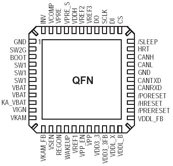
33394: Features: • Wide operating input voltage range: +4.0V to +26.5V (+45V transient).• Provides all regulated voltages for MPC5XX MCUs and other ECU's logic and analog functions.• Accu...

floor Price/Ceiling Price

Part Number:
33394
Supply Ability:
5000

Price Break

  • Qty
  • 1~5000
  • Unit Price
  • Negotiable
  • Processing time
  • 15 Days
Total Cost: $ 0.00

SeekIC Buyer Protection PLUS - newly updated for 2013!

  • Escrow Protection.
  • Guaranteed refunds.
  • Secure payments.
  • Learn more >>

Month Sales

268 Transactions

Rating

evaluate  (4.8 stars)

Upload time: 2024/4/25

Payment Methods

All payment methods are secure and covered by SeekIC Buyer Protection PLUS.

Notice: When you place an order, your payment is made to SeekIC and not to your seller. SeekIC only pays the seller after confirming you have received your order. We will also never share your payment details with your seller.
Product Details

Description


Features:

• Wide operating input voltage range: +4.0V to +26.5V (+45V transient).
• Provides all regulated voltages for MPC5XX MCUs and other ECU's logic and analog functions.
• Accurate power up/down sequencing.
• Provides necessary MCU support monitoring and failsafe support.
• Provides three 5.0 V buffer supplies for internal & external (shortcircuit protected) sensors.
• Includes stepdown/stepup switching regulator to provide supply voltages during different battery conditions.
• Interfaces Directly to Standard 5.0V I/O for CMOS Microprocessors by means of Serial Peripheral Interface.


Pinout

  Connection Diagram


Specifications

Parameter
Min.
Max.
Unit
Supply Voltage (VBAT), Load Dump
Supply Voltage (KA_VBAT, VIGN), Load Dump
Supply Voltages (VDDH, VPP, VDD3_3, VDDL, VKAM)
Supply Voltages (VREF1, VREF2, VREF3, VSEN)
CANL, CANH (0<VBAT<18 VDC no time limit)
0.3
18
0.3
2.0
18
+45
+45
+5.8
+18
+26.5
V
V
V
V
V
ESD Voltage
Human Body Model all pins
Machine Model all pins
CANLesd, CANHesd
CANLesd, CANHesd
CANLtransient, CANHtransient
(Note 1)
(Note 2)
(Note 1)
(Note 2)
(Note 3)
2.0
200
4.0
200
200
+2.0
+200
+4.0
+200
+200
kV
V
kV
V
V
/SLEEP
REGON, VPP_EN, /HRESET, /PORESET, /PRERESET, HRT, DO, DI, CS, SCLK
CANTXD, CANRXD
Operational Package Temperature [Ambient Temperature]
Storage Temperature
 
18
0.3
0.3
40
65
+45
+7.0
+7.0
+125
+150
V
V
V
°C
°C
Power Dissipation (TA = 125C)
44 HSOP
44 QFN
54 SOICWEP
Lead Soldering Temperature
Maximum Junction Temperature
RJA, Thermal Resistance, Junction to Ambient (44 HSOP)
RJC, Thermal Resistance, Junction to Case (44 HSOP)
RJB, Thermal Resistance, Junction to Base (44 HSOP)
RJA, Thermal Resistance, Junction to Ambient (44 QFN)
RJC, Thermal Resistance, Junction to Case (44 QFN)
RJB, Thermal Resistance, Junction to Base (44 QFN)
RJA, Thermal Resistance, Junction to Ambient (54 SOICWEP)
RJC, Thermal Resistance, Junction to Case (54 SOICWEP)
RJB, Thermal Resistance, Junction to Base (54 SOICWEP)
(Note 4)
(Note 4)
(Note 4)
(Note 5)


(Note 6)
(Note 7)
(Note 8)
(Note 6)
(Note 7)
(Note 8)
(Note 6)
(Note 7)
(Note 8)
8.3
5.0
5.0
260
+150
41
0.2
3
77
1.7
5.0
52
1.2
8.1
W
W
W
°C
°C
°C/W
°C/W
°C/W
°C/W
°C/W
°C/W
°C/W
°C/W
°C/W

1. Human body model: C = 100 pF, R = 1.5 k .
2. Machine model: C = 200 pF, R = 10 W and L = 0.75 mH. In case of a discharge from pin CANL to pin GND: 100 V < CANL transient < +100 V; in case of a discharge from pin CANH to Vcc: 150 V < CANH transient < +150 V.
3. The waveforms of the applied transients is in accordance with "ISO 7637 part 1" test pulses 1, 2, 3a and 3b.
4. Maximum power dissipation at indicated junction temperature.
5. Lead soldering temperature limit is for 10 seconds maximum duration; contact Motorola Sales Office for device immersion soldering time/temperature limits.
6. Thermal resistance measured in accordance with EIA/JESD512.
7. Theoretical thermal resistance from the die junction to the exposed pad.
8. Thermal resistance measured in accordance with JESD518.


Description

The 33394 is a multioutput power supply integrated circuit with high speed CAN transceiver. The IC incorporates a switching preregulator operating over a wide input voltage range from +4.0V to +26.5V (with transients up to 45V).

The switching regulator has an internal 3.0A current limit and runs in both buck mode or boost mode to always supply a preregulated output followed by Low Drop Out (LDO) regulators: VDDH / 5.0V @ 400mA; VDD3_3 / 3.3V @ 120mA; VDDL / 2.6V (User scalable between 3.3V 1.25V) @ 400mA typically, using an external NPN pass transistor. The Keep Alive regulator VKAM (scalable) @ 50mA; FLASH memory programming voltage VPP / 5.0V or 3.3V @ 150mA; three sensor supply outputs VREF(1,2,3) / 5.0V (tracking VDDH) @ 100mA each; and a switched battery output (VSEN) to supply 125mA clamped to 17V.

Additional features include Active Reset circuitry watching VDDH, VDD3_3, VDDL and VKAM, user selectable Hardware Reset Timer (HRT), Power Sequencing circuitry guarantees the core supply voltages never exceed their limits or polarities during system power up and power down.

A high speed CAN transceiver physical layer interfaces between the microcontroller CMOS outputs and differential bus lines. The CAN driver is short circuit protected and tolerant of loss of battery or ground conditions.

33394 is designed specifically to meet the needs of modules, which use the MPC565 microcontroller, though it will also support others from the MPC5XX family of Motorola microcontrollers.


Customers Who Bought This Item Also Bought

Margin,quality,low-cost products with low minimum orders. Secure your online payments with SeekIC Buyer Protection.
Motors, Solenoids, Driver Boards/Modules
Resistors
Static Control, ESD, Clean Room Products
Soldering, Desoldering, Rework Products
Semiconductor Modules
View more