54FCT377

Features: Clock enable for address and data synchronization applicationsEight edge-triggered D flip-flops Buffered common clockSee 'FCT273 for master reset versionSee 'FCT373 for transparent latch versionSee 'FCT374 for TRI-STATE(R) versionTTL input and output level compatibleCMOS power consumptio...

product image

54FCT377 Picture
SeekIC No. : 004233371 Detail

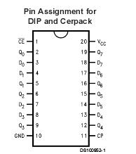
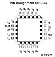
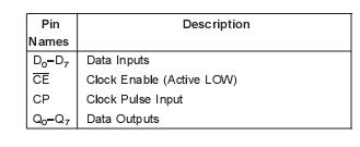
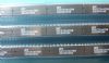
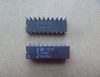
54FCT377: Features: Clock enable for address and data synchronization applicationsEight edge-triggered D flip-flops Buffered common clockSee 'FCT273 for master reset versionSee 'FCT373 for transparent latch v...

floor Price/Ceiling Price

Part Number:
54FCT377
Supply Ability:
5000

Price Break

  • Qty
  • 1~5000
  • Unit Price
  • Negotiable
  • Processing time
  • 15 Days
Total Cost: $ 0.00

SeekIC Buyer Protection PLUS - newly updated for 2013!

  • Escrow Protection.
  • Guaranteed refunds.
  • Secure payments.
  • Learn more >>

Month Sales

268 Transactions

Rating

evaluate  (4.8 stars)

Upload time: 2025/12/25

Payment Methods

All payment methods are secure and covered by SeekIC Buyer Protection PLUS.

Notice: When you place an order, your payment is made to SeekIC and not to your seller. SeekIC only pays the seller after confirming you have received your order. We will also never share your payment details with your seller.
Product Details

Description


Features:

Clock enable for address and data synchronization applications
Eight edge-triggered D flip-flops Buffered common clock
See 'FCT273 for master reset version
See 'FCT373 for transparent latch version
See 'FCT374 for TRI-STATE(R) version
TTL input and output level compatible
CMOS power consumption
Output sink capability of 32 mA, source capability of 12 mA
Standard Microcircuit Drawing (SMD) 5962-8762701


Pinout

  Connection Diagram  Connection Diagram  Connection Diagram


Specifications

Storage Temperature ...................................................-65 to +150
Ambient Temperature under Bias................................. -55 to +125
Junction Temperature under Bias
    Ceramic ....................................................................-55 to +175
VCC Pin Potential to
    Ground Pin .................................................................-0.5V to +7.0V
Input Voltage (Note 2) ...................................................-0.5V to +7.0V
Input Current (Note 2) .............................................-30 mA to +5.0 mA
Voltage Applied to Any Output
    in the Disabled or
    Power-Off State .......................................................-0.5V to +4.75V
    in the HIGH State .........................................................-0.5V to V CC
Current Applied to Output
    in LOW State (Max) ....................................Twice the rated IOL (mA)
DC Latchup Source Current...................................................... -500 mA
(Across Comm Operating Range)


Description

The 54FCT377 has eight edge-triggered, D-type flip-flops with individual D inputs and Q outputs. The common buffered
Clock (CP) input loads all flip-flops simultaneously, when the Clock Enable (CE) is LOW.

The register 54FCT377 is fully edge-triggered. The state of each D in-put, one setup time before the LOW-to-HIGH clock transi-
tion, is transferred to the corresponding flip-flop's Q output. The CE input of 54FCT377 must be stable only one setup time prior to the LOW-to-HIGH clock transition for predictable operation.


Customers Who Bought This Item Also Bought

Margin,quality,low-cost products with low minimum orders. Secure your online payments with SeekIC Buyer Protection.
Potentiometers, Variable Resistors
Test Equipment
Semiconductor Modules
Power Supplies - Board Mount
Prototyping Products
DE1
Boxes, Enclosures, Racks
View more