Features: • Fast access times: 7.5, 8, 8.5, and 10ns
• Fast clock speed: 117, 100, 90, and 50 MHz
• Provide high performance 2-1-1-1 access rate
• Fast OE# access times: 4.0ns
• 3.3V -5% and +10% power supply
• 5V tolerant inputs except I/O's
• Clamp diodes to VSSQ at all inputs and outputs
• Common data inputs and data outputs
• BYTE WRITE ENABLE and GLOBAL WRITE control
• Three chip enables for depth expansion and address pipeline
• Address, data and control registers
• Internally self-timed WRITE CYCLE
• Burst control pins (interleaved or linear burst sequence)
• Automatic power-down for portable applications
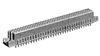
• High density, high speed packagesPinout Specifications
Voltage on VCC Supply Relative to VSS..... .-0.5V to +4.6V
VIN .........................................................-0.5V to VCC+0.5V
Storage Temperature (plastic) ....................-55oC to +125o
Junction Temperature ................................................+125o
Power Dissipation .......................................................1.6W
Short Circuit Output Current (per I/O).........................20mA
*Stresses greater than those listed under "Absolute Maximum Ratings" may cause permanent damage to the device.This is a stress rating only and functional operation of the device at these or any other conditions above those indicated in the operational sections of this specification is not implied. Exposure to absolute maximum rating conditions for extended periods may affect reliability.
DescriptionThe Galvantech Synchronous Burst SRAM family mploys high-speed, low power CMOS designs using advanced triple-layer polysilicon, double-layer metal techn logy. Each memory cell consists of four transistors and two high valued resistors.
The 6504 SRAM integrates 131,072x36 SRAM cells with advanced synchronous peripheral circuitry and a 2-bit counter for internal burst operation. All synchronous inputs are gated by registers controlled by a positive-edge-triggered clock input (CLK). The synchronous inputs include all addresses, all data inputs, address-pipelining chip enable (CE#), depth-expansion chip enables (CE2# and CE2), burst control inputs (ADSC#, ADSP#, and ADV#), write enables (BW1#, BW2#, BW3#, BW4#,and BWE#), and global write (GW#).
Asynchronous inputs include the output enable (OE#), burst mode control (MODE), and sleep mode control (ZZ). The data outputs (Q), enabled by OE#, are also asynchronous. Addresses and chip enables are registered with either address status processor (ADSP#) or address status controller (ADSC#) input pins. Subsequent burst addresses can be internally generated as controlled by the burst advance pin (ADV#).
Address, data inputs, and write controls are registered onchip to initiate self-timed WRITE cycle. WRITE cycles can be one to four bytes wide as controlled by the write control inputs. Individual byte write allows individual byte to be written. BW1# controls DQ1-DQ8 and DQP1. BW2# controls DQ9-DQ16 and DQP2. BW3# controls DQ17-DQ24 and DQP3. BW4# controls DQ25-DQ32 and DQP4. BW1#,BW2# BW3#, and BW4# can be active only with BWE# being LOW. GW# being LOW causes all bytes to be written.
The 6504 operates from a +3.3V core power supply and all outputs operate on a +2.5V supply. All inputs and outputs are JEDEC standard JESD8-5 compatible. The device is ideally suited for 486, PentiumTM, 680x0, and PowerPCTM systems and for systems that are benefited from a wide synchronous data bus

 6504 Data Sheet