Features: `Low Power Monolithic 128K x 8 FLASH
`TTL Compatible Inputs and CMOS Outputs
`Access Times of 60, 70, 90, 120 and 150ns
`+5V Programing, +5V Supply
`100,000 Erase / Program Cycles
`Low Standby Current
`Page Program Operation and Internal Program Control Time
`Supports Full Chip Erase
`Embedded Erase and Program Algorithms
`Supports Full Chip Erase
`MIL-PRF-38534 Compliant Circuits Available
`Industry Standard Pinouts
`Packaging Hermetic Ceramic
.32 Lead, 1.6" x .6" x .20" Dual-in-line Package (DIP), Aeroflex code# "P4"
.32 Lead, .82" x .41" x .125" Ceramic Flat Package (FP), Aeroflex code# "F6"
.32 Lead, .82" x .41" x .132" Ceramic Flat Package (FP Lead Formed), Aeroflex code# "F7"
`Sector Architecture
.8 Equal size sectors of 16K bytes each
.Any Combination of Sectors can be erased with one command sequence.
`Commercial, Industrial and Military Temperature Ranges
`DESC SMD Pending 5962-96690 (P4,F6,F7)Pinout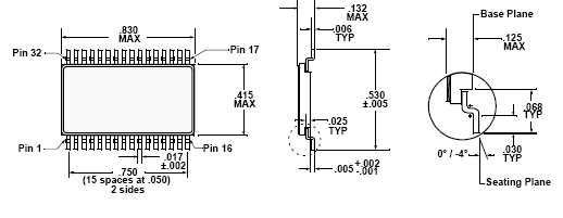 Specifications
| Parameter |
Symbol |
Range |
Units |
| Case Operating Temperature |
TC |
-55 to +125 |
°C |
| Storage Temperature Range |
TSTG |
-65 to +150 |
°C |
| Supply Voltage Range |
VCC |
-2.0 to +7.0 |
V |
| Signal Voltage Range (Any Pin Except A9) Note 1 |
VG |
-2.0 to +7.0 |
V |
| Maximum Lead Temperature (10 seconds) |
|
300 |
°C |
| Data Retention |
|
10 |
Years |
| Endurance (Write/Erase cycles) |
|
100,000 Minimum |
|
| A9 Voltage for sector protect, Note 2 |
VID |
-2.0 to +14.0 |
V |
Descriptionhermetically sealed ceramic packages; a 32 lead .82" x .41" x .125" flat package in both formed or unformed leads or a 32 pin 1.6"x.60" x.20" DIP package for operation over the temperature range -55°C to +125°C and military environmental conditions. The flash memory is organized as 128Kx8 bits and is designed to be programmed in-system with the standard system 5.0V Vcc supply. A 12.0V VPP is not required for write or erase operations.
The device ACTF128K8 can also be reprogrammed with standard EPROM programmers (with the proper socket). The standard ACTF128K8 offers access times between 60ns and 150ns, allowing operation of high-speed microprocessors without wait states. To eliminate bus contention, the device has separate chip enable (CE), write enable (WE) and output enable (OE) controls.
The ACTF128K8 is command set compatible with JEDEC standard 1 Mbit EEPROMs. Commands are written to the command register using standard microprocessor write timings. Register contents serve as input to an internal state-machine which controls the erase and programming circuitry. Write cycles also internally latch addresses and data needed for the programming and erase operations.
Reading data out of the device ACTF128K8 is similar to reading from 12.0V Flash or EPROM devices. The ACTF128K8 is programmed by executing the program command sequence. This will invoke the Embedded Program Algorithm which is an internal algorithm that automatically times the program pulse widths and verifies proper cell margin. Typically, each sector can be programmed and verified in less than 0.3 second. Erase is accomplished by executing the erase command sequence. This will invoke the Embedded Erase Algorithm which is an internal algorithm that automatically preprograms the array, (if it is not already programmed before) executing the erase operation. During erase, the device automatically times the erase pulse widths and verifies proper cell margin.
Also the device ACTF128K8 features a sector erase architecture. The sector mode allows for 16K byte blocks of memory to be erased and reprogrammed without affecting other blocks. The ACT-F128K8 is erased when shipped from the factory.
The device features single 5.0V power supply operation for both read and write functions. lnternally generated and regulated voltages are provided for the program and erase operations. A low VCC detector automatically inhibits write operations on the loss of power. The end of program or erase is detected by Data Polling of D7 or by the Toggle Bit feature on D6. Once the end of a program or erase cycle has been completed, the device internally resets to the read mode.
All bits of each die, or all bits within a sector of a die, are erased via Fowler-Nordhiem tunneling. Bytes are programmed one byte at a time by hot electron injection. A DESC Standard Military Drawing (SMD) number is pending.

 ACTF128K8 Data Sheet


