Features: `4 Low Voltage/Power Intel 1M x 8 FLASH Die in One MCM Package
`Overall Configuration is 1M x 32
`+5V Operation (Standard) or +3.3V (Consult Factory)
`Access Times of 80, 100 and 120 nS ( 5V VCC)
`+5V or +12V Programing
`Erase/Program Cycles
. 100,000 Commercial
. 10,000 Military and Industrial
`Sector Architecture (Each Die)
. One 16K Protected Boot Block (Bottom Boot Block Standard, Top Boot Block Special Order)
. Two 8K Parameter Blocks
. One 96K Main Block
. Seven 128K Main Blocks
`Single Block Erase (All bits set to 1)
`Hardware Data Protection Feature
`Independent Boot Block Locking
`MIL-PRF-38534 Compliant MCMs Available
`Packaging Hermetic Ceramic
. 68 Lead, .94" x .94" x .180" Dual-Cavity Small Outline Gull Wing, Aeroflex code# "F14" (Drops into the 68 Lead JEDEC .99"SQ CQFJ footprint)
`Internal Decoupling Capacitors for Low Noise Operation
`Commercial, Industrial and Military Temperature RangesPinout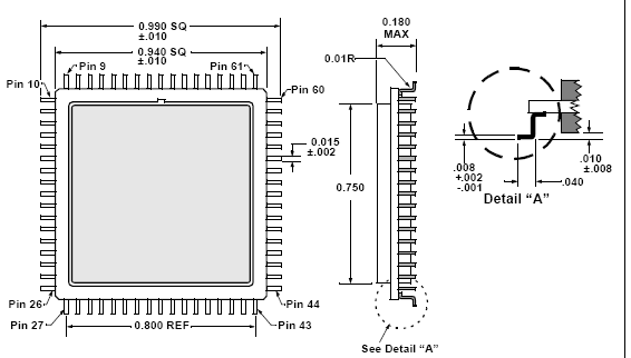 Specifications
| Parameter |
Range |
Units |
| Case Operating Temperature Range |
-55 to +125 |
°C |
| Storage Temperature Range |
-65 to +150 |
°C |
| Voltage on Any Pin with Respect to GND (except VCC, VPP, A9 and RP) (1) |
-2.0 to +7.0 |
V |
| Voltage on Pins A9 or RP with Respect to GND (except VCC, VPP, A9 and RP) (1,2) |
-2.0 to +13.5 |
V |
| VPP Program Voltage with Respect to GND during Block Erase/ and Word/Byte Write (1,2) |
-2.0 to +14.0 |
V |
| Vcc Supply Voltage with Respect to Ground (1) |
-2.0 to +7.0 |
V |
| Output Short Circuit Current (3) |
100 |
mA |
Descriptionaccomplished by chip Enable (CE) and Output Enable (OE) being logically active. Access time grades of 80nS, 100nS and 120nS maximum are standard.
The ACTF1M32 is packaged in a hermetically sealed co-fired ceramic 68 lead, .94" SQ Ceramic Gull Wing CQFP package. This allows operation in a military environment temperature range of -55°C to +125°C.
The ACTF1M32 provides program and erase capability at 5V or 12V and allows reads with Vcc at 5V or 3.3V(Not tested). Since many designs read from flash memory a large percentage of the time, read operation using 3.3V can provide great power savings. Consult the factory for 3.3V tested parts. In applications where read performance is critical, faster access times are obtainable with the 5V VCC part detailed herein. For program and erase operations, 5V Vpp operation eliminates the need for in system voltage converters. The 12V Vpp operation provides reduced (approx 60%) program and erase times where 12V is available in the system.
For design simplicity, however, connect Vcc and Vpp to the same 5V ±10% source. Each block of ACTF1M32 can be independently erased and programmed 100,000 times at commercial temperature or 10,000 times at extended temperature. The boot block is located at either the bottom (Standard) or the top (Special Order) of the address map in order to accommodate different microprocessor protocols for boot code location. Locking and unlocking of the boot block is controlled by WP and/or RP.
Intel's boot block architecture provides a flexible solution for the different design needs of various applications. The asymmetrically-blocked memory map allows the integration of several memory components into a single flash device. The boot block provides a secure boot PROM; the parameter blocks can emulate EEPROM functionality for parameter store with proper software techniques; and the main blocks provide code and data storage with access times fast enough to execute code in place, decreasing RAM requirements.
For Detail Information regarding the operation of the 28F800BV Memory die, see the Intel datasheet (order number 290539-002).

 ACTF1M32 Data Sheet


