Features: ·40-channel DAC in 64 Lead LFCSP and LQFP
·Guaranteed monotonic to 16 bits
·Maximum output voltage span of 4 × VREF (20 V)
·Nominal output voltage range of -4 V to +8 V
·Multiple, independent output span available
·System calibration function allowing user-programmable offset and gain
·Clear function to user-defined SIGGND (CLR pin)
·Simultaneous update of DAC outputs (LDAC pin)
·Channel grouping and addressing features
·Thermal Monitor Function
·DSP/microcontroller-compatible serial interface
·2.5 V to 5.5 V JEDEC-compliant digital levels
·Power-on reset
·Digital reset (RESET)Application·Level setting in automatic test equipment (ATE)
·Variable optical attenuators (VOA)
·Optical switches
·Industrial control systems
·InstrumentationPinout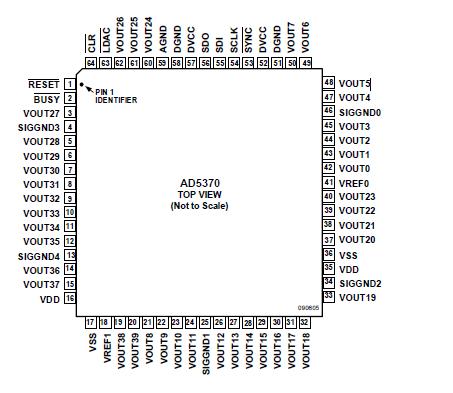 Specifications
VDD to AGND...............................−0.3 V to +17 V
VSS to AGND...............................−17 V to +0.3 V
VCC to DGND................................−0.3 V to +7 V
Digital Inputs to DGND......−0.3 V to VCC + 0.3 V
Digital Outputs to DGND...−0.3 V to VCC + 0.3 V
VREF1(+), VREF2(+) to AGND.......−0.3 V to +7 V
VREF1(−), VREF2(−) to AGND..VSS− 0.3 V to VDD + 0.3 V
VBIAS to AGND.............................−0.3 V to +7 V
VOUT0VOUT31 to AGND......VSS − 0.3 V to VDD + 0.3 V
REFGND to AGND..................VSS − 0.3 V to VDD + 0.3 V
AGND to DGND.........................−0.3 V to +0.3 V
Operating Temperature Range (TA)
Industrial (A Version)...........................−40°C to +85°C
Storage Temperature Range.............−65°C to +150°C
Junction Temperature (TJ max)............................130°C
108-Lead CSPBGA Package
JA Thermal Impedance
64-LFCSP ............................................25°C/W
64-LQFP ..........................................45.5°C/W
Reflow Soldering
Peak Temperature.....................................230°C
Time at Peak Temperature..........10 sec to 40 sec
Stresses above those listed under Absolute Maximum Ratings may cause permanent damage to the device. This is a stress rating only, and functional operation of the device at these or any other conditions above those listed in the operational sections of this specification is not implied. Exposure to absolute maximum rating conditions for extended periods may affect device reliability.
DescriptionThe AD5370 contains 40, 16-bit DACs in a single, 64-lead,LFCSP or LQFP package. The AD5370 provides buffered voltage outputs with a span 4 times the reference voltage. The gain and offset of each DAC can be independently trimmed to remove errors. For even greater flexibility, the device is divided into 5 groups of 8 DACs. Two offset DACs allow the output range of the groups to be altered.
The AD5370 offers guaranteed operation over a wide supply range with VSS from -4.5V to -16.5 V and VDD from +8 V to +16.5 V. The output amplifier headroom requirement is 1.4 V operating with a load current of 1 mA.
The AD5370 has a high-speed serial interface, which is compatible with SPI®, QSPI™, MICROWIRE™, and DSP interface standards and can handle clock speeds of up to 50 MHz.
The DAC AD5370 outputs are updated on reception of new data into the DAC registers. All the outputs can be updated simultaneously by taking the LDAC input low. Each channel has a programmable gain and an offset adjust register.
Each DAC AD5370 output is gained and buffered on-chip with respect to an external SIGGND input. The DAC outputs can also be switched to SIGGND via the CLR pin.

 AD5370 Data Sheet