Features: Complete ATM Transceiver for 155 Mbps for UTP#5 or Fiber
Meets ATM Forum UNI 3.1 Requirements
Meets SONET/SDH Jitter Requirements
Meets FCC Class B Emissions Requirements
Drives up to 110M Category #5 UTP/FTP
Adjustable Line Driver Output Current
Equalizes up to 110M Category #5 UTP/FTP
Baseline Restoration Function Eliminates Baseline Wander
19.44 MHz Oscillator Circuit
Frequency Synthesizer for 155 MHz Tx Bit Clock
155 Mbps Clock Recovery and Data Retiming
Phase Continuous Switch at Frequency Synthesizer Output
Single Supply Operation: +5 V or 5.2 V
Low Power: 400 mW
10KH ECL Compatible Output
Package: 44-Pin Thin Quad FlatpackApplicationApplication with Fiber Optic Receivers/Transceivers
The AD6816 receiver (adaptive equalizer and baseline restore loop) can be configured to receive a signal from a fiber optic receiver or transceiver that provides full PECL or ECL outputs. By properly adjusting the common mode and amplitude level, the AD6816 receiver will be essentially transparent to the (P)ECL inputs. The common-mode input voltage should be between 1.5 V and 1.9 V referred to VCC. The differential input amplitude should be between 0.7 V and 1.1 V. The commonmode issue can be addressed simply by ac coupling. The amplitude of the (P)ECL signal should be attenuated by two to meet the above requirement.
Figure 18 provides a simple solution that satisfies the above requirements as well as providing proper 50 W terminations for transmission lines when needed. The circuit also allows a convenient way to double pad a PC board for either fiber or copper cable applications.
Pinout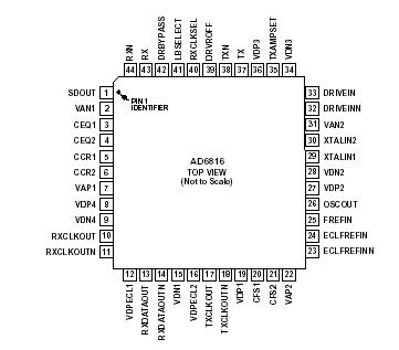 SpecificationsSupply Voltage . . . . . . . . . . . . . . . . . . . . . . . . . . . . . . +12 V
Input Voltage (Pin 43 or Pin 44 to VCC) . . . . . . VCC + 0.6 V
Maximum Junction Temperature . . . . . . . . . . . . . . .+165°C
Storage Temperature Range . . . . . . . . 65°C to +150°C
Lead Temperature Range (Soldering 10 sec) . . . . .+300°C
ESD Rating (Human Body Model) . . . . . . . . . . . . . . . 1500 VDescriptionThe AD6816 provides a single chip solution for interfacing an ATM User-Network Interface IC to either a Category #5 Unshielded Twisted Pair (UTP) system or a fiber optic system. The IC provides line equalization and baseline restoration, line driver, clock recovery and data retiming, local reference clock oscillator and frequency synthesis functions. Signal multiplexers within the IC allow the user to perform loop-back, bypass the data retiming function and select the frequency reference for the transmit bit clock (independent timing or loop timing).
The line equalization and baseline restoration block compensates for up to 110M Category #5 UTP and transformer, respectively. This block has a Signal Detect output, SDOUT, that when low indicates a loss of input signal at RX, RXN. The AD6816 supports application with a fiber optic receiver or transceiver. In this case, the line equalizer block adapts to provide no equalization.
The line driver AD6816 has a differential ECL input stage providing controlled current output suitable for driving a Category #5 UTP system. A single resistor from the line driver output current control pin to ground controls the output current. The user has the option to disable the line driver output. A signal multiplexer allows the user to loop back the line driver input signal through the clock recovery and data retiming PLL for test purposes.
The clock recovery and data retiming PLL of AD6816 has a factory trimmed VCO center frequency and an integrated frequency control loop that combine to ensure signal acquisition. This eliminates reliance on external components, like a crystal or an SAW filter, to aid frequency acquisition. At frequency lock, the frequency error is zero and the frequency detector has no effect. At this point, the PLL works to ensure that the output phase tracks the input Information furnished by Analog Devices is believed to be accurate and reliable. However, no responsibility is assumed by Analog Devices for its use, nor for any infringements of patents or other rights of third parties which may result from its use. No license is granted by implication or otherwise under any patent or patent rights of Analog Devices.

 AD6816 Data Sheet