Features: Single Chip Solution, Contains Internal Oscillator and
Voltage Reference
No Adjustments Required
Interfaces to Half-Bridge, 4-Wire LVDT
DC Output Proportional to Position
20 Hz to 20 kHz Frequency Range
Unipolar or Bipolar Output
Will Also Decode AC Bridge Signals
Outstanding Performance
Linearity: 0.05%
Output Voltage: 11 V
Gain Drift: 20 ppm/C (typ)
Offset Drift: 5 ppm/C (typ)ApplicationMost of the applications for the AD598 can also be imple-mented with the AD698. Please refer to the applications written or the AD598 for a detailed explanation.
See AD598 data sheet for:
Proving Ring-Weigh Scale
Synchronous Operation of Multiple LVDTs
High Resolution Position-to-Frequency Circuit Low Cost Setpoint Controller
Mechanical Follower Servo Loop
Differential Gaging and Precision Differential Gaging
Pinout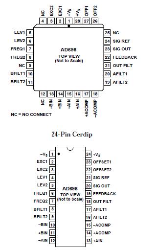 SpecificationsSupply Voltage (+VS to VS) . . . . . . . . . . . . . . . . .. . ..36 V
Storage Temperature Range
P Package . . . . . . . . . . . . . . . . . . . . . . . . .65°C to +150°C
Q Package . . . . . . . . . . . . . . . . . . . . . . . . 65°C to +150°C
Operating Temperature Range
AD698SQ . . . . . . . . . . . . . . . . . . . . . . . .. .55°C to +125°C
AD698AP . . . . . . . . . . . . . . . . . . . . . . . . .. . 40°C to +85°C
Lead Temperature Range (Soldering 60 sec) . . . . . . +300°C
Power Dissipation Derates above +65°C
P Package . . . . . . . . . . . . . . . . . . . . . . . . . . . . . . . 12 mW/ C
°
Q Package . . . . . . . . . . . . . . . . . . . . . . . . . . . . . . 12 mW/°CDescriptionThe AD698 is a complete, monolithic Linear Variable Differen-tial Transformer (LVDT) signal conditioning subsystem. It is used in conjunction with LVDTs to convert transducer mechan-ical position to a unipolar or bipolar dc voltage with a high de-gree of accuracy and repeatability. All circuit functions are included on the chip. With the addition of a few external passive components to set frequency and gain, the AD698 converts the raw LVDT output to a scaled dc signal. The device will operate with half-bridge LVDTs, LVDTs connected in the series op-posed configuration (4-wire), and RVDTs.
The AD698 contains a low distortion sine wave oscillator to drive the LVDT primary. Two synchronous demodulation channels of the AD698 are used to detect primary and second-ary amplitude. The part divides the output of the secondary by the amplitude of the primary and multiplies by a scale factor.This eliminates scale factor errors due to drift in the amplitude of the primary drive, improving temperature performance and stability.
The AD698 uses a unique ratiometric architecture to eliminate everal of the disadvantages associated with traditional ap-proaches to LVDT interfacing.The benefits of this new cir-cuit are: no adjustments are necessary; temperature stability is improved; and transducer interchangeability is improved.
The AD698 is available in two performance grades:
Grade Temperature Range Package
AD698AP 40°C to +85°C 28-Pin PLCC
AD698SQ 55°C to +125°C 24-Pin Cerdip

 AD698 Data Sheet