AD7002

Features: Single +5 V SupplyTransmit ChannelOn-Chip GMSK ModulatorTwo 10-Bit D/A ConvertersAnalog Reconstruction FiltersPower-Down ModeReceive ChannelTwo Sigma-Delta A/D ConvertersFIR Digital FiltersOn-Chip Offset CalibrationPower-Down Mode3 Auxiliary D/A ConvertersPower-Down ModesOn-Chip Voltage ...

product image

AD7002 Picture
SeekIC No. : 004269836 Detail

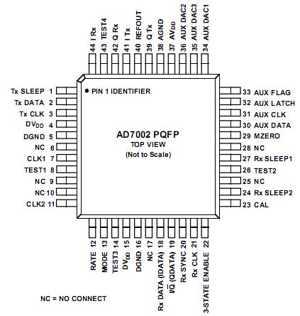
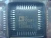
AD7002: Features: Single +5 V SupplyTransmit ChannelOn-Chip GMSK ModulatorTwo 10-Bit D/A ConvertersAnalog Reconstruction FiltersPower-Down ModeReceive ChannelTwo Sigma-Delta A/D ConvertersFIR Digital Filter...

floor Price/Ceiling Price

Part Number:
AD7002
Supply Ability:
5000

Price Break

  • Qty
  • 1~5000
  • Unit Price
  • Negotiable
  • Processing time
  • 15 Days
Total Cost: $ 0.00

SeekIC Buyer Protection PLUS - newly updated for 2013!

  • Escrow Protection.
  • Guaranteed refunds.
  • Secure payments.
  • Learn more >>

Month Sales

268 Transactions

Rating

evaluate  (4.8 stars)

Upload time: 2024/4/28

Payment Methods

All payment methods are secure and covered by SeekIC Buyer Protection PLUS.

Notice: When you place an order, your payment is made to SeekIC and not to your seller. SeekIC only pays the seller after confirming you have received your order. We will also never share your payment details with your seller.
Product Details

Description


Features:

Single +5 V Supply
Transmit Channel
On-Chip GMSK Modulator
Two 10-Bit D/A Converters
Analog Reconstruction Filters
Power-Down Mode
Receive Channel
Two Sigma-Delta A/D Converters
FIR Digital Filters
On-Chip Offset Calibration
Power-Down Mode
3 Auxiliary D/A Converters
Power-Down Modes
On-Chip Voltage Reference
Low Power
44-Lead PQFP


Application

GSM
PCN


Pinout

  Connection Diagram


Specifications

DVDD to AGND  . . . . . . . . . . . . . . . . . . . . . . . 0.3 V to +7 V
AVDD to AGND  . . . . . . . . . . . . . . . . . . . . . . . 0.3 V to +7 V
AGND to DGND  . . . . . . . . . . . . . . . . . . . .    0.3 V to +0.3 V
Digital Input Voltage to DGND  . . . .  0.3 V to DVDD + 0.3 V
Analog Input Voltage to AGND  . . . . 0.3 V to AVDD + 0.3 V
Input Current to Any Pin Except Supplies2. . . . . . . .±10 mA
Operating Temperature Range
Industrial Plastic (A Version)  . . . . . . . . . . .40°C to +85°C
Storage Temperature Range  . . . . . . . . . 65°C to +150°C
Lead Temperature (Soldering, 10 secs)  . . . . . . . .  +300°C
Power Dissipation (Any Package) to +75°C  . . . . . 450 mW
Derates Above +75°C by  . . . . . . . . . . . . . . . . . .10 mW/°C


Description

The AD7002 is a complete low power, two-channel, input/ output port with signal conditioning. The device is used as a baseband digitization subsystem, performing signal conversion between the DSP and the IF/RF sections in the Pan-European telephone system (GSM). The transmit path consists of an onboard digital modulator, containing all the code necessary for performing Gaussian Minimum Shift Keying (GMSK), two high accuracy, fast DACs with output reconstruction filters. The receive path is composed of two high performance sigma-delta ADCs with digital filtering. A common bandgap reference feeds the ADCs and signal DACs.

Three control DACs (AUX DAC1 to AUX DAC3) are included for such functions as AFC, AGC and carrier signal shaping. In addition, AUX FLAG may be used for routing digital control information through the device to the IF/RF sections. As it is a necessity for all GSM mobile systems to use the lowest power possible, the device has power-down or sleep options for all sections (transmit, receive and auxiliary). The AD7002 is housed in 44-lead PQFP (Plastic Quad Flatpack).


Customers Who Bought This Item Also Bought

Margin,quality,low-cost products with low minimum orders. Secure your online payments with SeekIC Buyer Protection.
Programmers, Development Systems
Integrated Circuits (ICs)
Prototyping Products
DE1
Hardware, Fasteners, Accessories
Semiconductor Modules
Audio Products
View more