Features: Single +5 V Supply
Receive Channel
Differential or Single-Ended Analog Inputs
Auxiliary Set of Analog I & Q Inputs
Two Sigma-Delta A/D Converters
Choice of Two Digital FIR Filters
Root-Raised-Cosine Rx Filters, = 0.35
Brick Wall FIR Rx Filters
On-Chip or User Rx Offset Calibration
ADC Sampling Vernier
Three Auxiliary DACs
On-Chip Voltage Reference
Low Active Power Dissipation, Typical 45 mW
Low Sleep Mode Power Dissipation, <50 µW
28-Pin SSOPApplicationAmerican TIA Digital Cellular Telephony
American Analog Cellular Telephony
Digital Baseband ReceiversPinout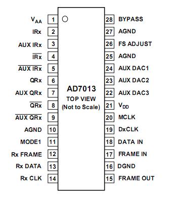 Specifications(TA = +25°C unless otherwise noted)
VAA, VDD to GND .................................................0.3 V to +7 V
AGND to DGND ........................ .................... ...0.3 V to +0.3 V
Digital I/O Voltage to DGND ........... ..........0.3 V to VDD +0.3 V
Analog I/O Voltage to AGND .....................0.3 V to VDD +0.3 V
Operating Temperature Range
Industrial (A Version) ................... .................40°C to +85°C
Storage Temperature Range .......................65°C to +150°C
Maximum Junction Temperature ............................. +150°C
SSOP JA Thermal Impedance .............................. +122°C/W
Lead Temperature Soldering
Vapor Phase (60 sec) ............................................... +215°C
Infrared (15 sec) .................................................. +220°C
NOTES
1
Stresses above those listed under "Absolute Maximum Ratings" may cause permanent damage to the device. This is a stress rating only and functional operation of the device at these or any other conditions above those listed in the operational sections of this specification is not implied. Exposure to absolute maximum rating conditions extended periods may affect device reliability.DescriptionThe AD7013 is a complete low power, CMOS, TIA IS-54 baseband receive port with single +5 V power supply. The part is designed to perform the baseband conversion of I and Q waveforms in accordance with the American (TIA IS-54) Digital Cellular Telephone system.
The receive path AD7013 consists of two high performance sigma-delta ADCs, each followed by a FIR digital filter. A primary and auxiliary set of IQ differential analog inputs are provided,where either can be selected as inputs to the sigma-delta ADCs. Also, a choice of two frequency responses are available for the receive FIR filters; a Root-Raised-Cosine filter for digital mode or a brick wall response for analog mode.Differential analog inputs are provided for both I and Q channels. On-chip calibration logic is also provided to remove either on-chip offsets or remove system offsets. A 16-bit serial interface is provided, interfacing easily to most DSPs. The receive path also provides a means to vary the sampling instant, giving a resolution to 1/32 of a symbol interval.
The auxiliary section AD7013 provides two 8-bit DACs and one 10-bit DAC for functions such as automatic gain control (AGC),
automatic frequency control (AFC) and power amplifier control.
As AD7013 is a necessity for all digital mobile systems to use the lowest possible power, the device has receive and auxiliary power down options. The AD7013 is housed in a space efficient 28-pin SSOP (Shrink Small Outline Package).

 AD7013 Data Sheet