Features: 10-Bit Dual Transmit DAC 125 MSPS Update Rate Excellent SFDR and IMD: 78 dBc Excellent Gain and Offset Matching: 0.1% Fully Independent or Single Resistor Gain Control Dual Port or Interleaved Data On-Chip 1.2 V Reference Single 5 V or 3 V Supply Operation Power Dissipation: 380 mW @ 5 V Power-Down Mode: 50 mW @ 5 V 48-Lead LQFP
ApplicationCommunications Base Stations Digital Synthesis Quadrature Modulation
Pinout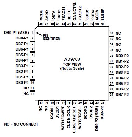
 Specifications
| Parameter |
With
Respect to |
Min |
Max |
Units |
|
AVDD
DVDD
ACOM
AVDD
MODE, CLK1, CLK2, WRT1, WRT2
Digital Inputs
IOUTA1/IOUTA2, IOUTB1/IOUTB2
REFIO, FSADJ1, FSADJ2
GAINCTRL, SLEEP
Junction Temperature
Storage Temperature
Lead Temperature (10 sec) |
ACOM
DCOM
DCOM
DVDD
DCOM
DCOM
ACOM
ACOM
ACOM |
0.3
0.3
0.3
6.5
0.3
0.3
1.0
0.3
0.3
65 |
+6.5
+6.5
+0.3
+6.5
DVDD + 0.3
DVDD + 0.3
AVDD + 0.3
AVDD + 0.3
AVDD + 0.3
+150
+150
+300 |
V
V
V
V
V
V
V
V
V
|
| Resolution (Bits) |
10bit |
| DAC Update Rate |
125MSPS |
| DAC Settling Time |
35ns |
| # DAC Outputs |
2 |
| DAC Type |
Current Out |
| DAC Input Format |
Par |
| Output FSR |
(Iout x Rload),Adj(Uni 2mA to Uni 20mA),User Def. Range/Offset |
| Ref Int/Ext |
Int/Ext |
| Supply Vnom |
Single(+5) |
| Pwr Diss |
450mW |
| Package |
QFP |
DescriptionThe AD9763 is a dual port, high speed, two-channel, 10-bit CMOS DAC. It integrates two high quality 10-bit TxDAC+ cores, a voltage reference and digital interface circuitry into a small 48-lead LQFP package. The AD9763 offers exceptional ac and dc performance while supporting update rates up to 125 MSPS.
The AD9763 has been optimized for processing I and Q data in communications applications. The digital interface consists of two double-buffered latches as well as control logic. Separate
write inputs allow data to be written to the two DAC ports independent of one another. Separate clocks control the update rate of the DACs.
A mode control pin allows the AD9763 to interface to two separate data ports, or to a single interleaved high speed data port. In interleaving mode the input data stream is demuxed into its original I and Q data and then latched. The I and Q data is then converted by the two DACs and updated at half the input data rate.
The GAINCTRL pin allows two modes for setting the full-scale current (IOUTFS) of the two DACs. IOUTFS for each DAC can be set independently using two external resistors, or IOUTFS for both DACs can be set by using a single external resistor.**
The DACs utilize a segmented current source architecture combined with a proprietary switching technique to reduce glitch energy and to maximize dynamic accuracy. Each DAC provides differential current output thus supporting single-ended or differential applications. Both DACs can be simultaneously updated and provide a nominal full-scale current of 20 mA. The full-scale currents between each DAC are matched to within 0.1%.
The AD9763 is manufactured on an advanced low cost CMOS process. It operates from a single supply of 3.0 V to 5.0 V and consumes 380 mW of power.

 AD9763 Data Sheet