Features: COMPLETE 12-BIT A/D CONVERTER WITH REFERENCE, CLOCK, AND 8-, 12-, or 16- BIT MICROPROCESSOR BUS INTERFACE
ALTERNATE SOURCE FOR HI774 A/D CONVERTER: 8.5s Conversion Time, 150ns Bus Access Time
FULLY SPECIFIED FOR OPERATION ON ±12V OR ±15V SUPPLIES
NO MISSING CODES OVER TEMPERATURE:
0°C to +75°C: ADC774J, K
55°C to +125°C: ADC774SH, THPinout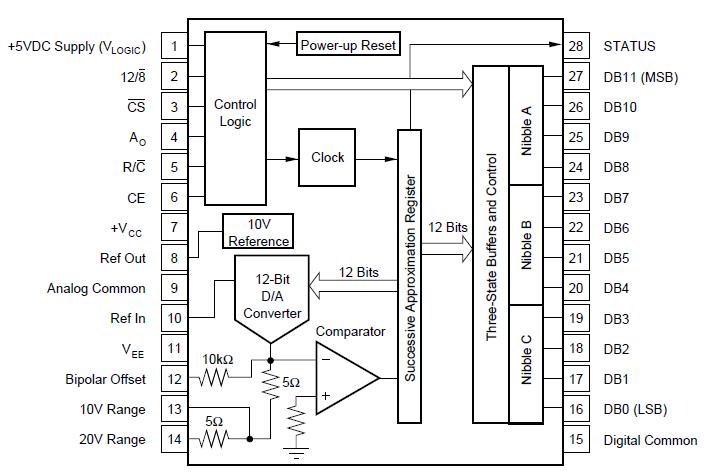 SpecificationsVCC to Digital Common ........................................................................ 0V to +16.5V
VEE to Digital Common ......................................................................... 0V to 16.5V
VLOGIC Digital Common ....................................................................... 0V to +7V
Analog Common to Digital Common .................................................... ±1V
Control Inputs (CE, CS, AO, 12/8, R/C)
to Digital Common .......................................................................... 0.5V to VLOGIC +0.5V
Analog Inputs (Ref In, Bipolar Offset, 10VIN )
to Analog Common ........................................................................ ±16.5V
20VIN to Analog Common .................................................................. ±24V
Ref Out .............................................................................................. Indefinite Short to Common,Momentary Short to VCC
Max Junction Temperature ................................................................ +165°C
Power Dissipation ............................................................................. 1000mW
Lead Temperature (soldering,10s) ................................................... +300°C
Thermal Resistance, JA : Ceramic ................................................... 50°C/W
Plastic ..................................................... 100°C/W
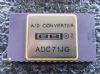
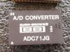
CAUTION: These devices are sensitive to electrostatic discharge. Appropriate I.C. handling procedures should be followed.DescriptionThe ADC774 is a 12-bit successive approximation analog-to-digital converter, utilizing state-of-the-art CMOS and laser-trimmed bipolar die custom-designed for freedom from latch-up and for optimum AC performance. It is complete with a self-contained +10V reference, internal clock, digital interface for microprocessor control, and three-state outputs.
The ADC774 reference circuit, containing a buried zener, is lasertrimmed for minimum temperature coefficient. The clock oscillator is current-controlled for excellent stability over temperature. Full-scale and offset errors may be externally trimmed to zero. Internal scaling resistors are provided for the selection of analog input signal ranges of 0V to +10V, 0V to +20V, ±5V, and ±10V.
The converter ADC774 may be externally programmed to provide 8- or 12-bit resolution. The conversion time for 12 bits is factory set for 8.5ms maximum.
Output data of ADC774 are available in a parallel format from TTLcompatible three-state output buffers. Output data are coded in straight binary for unipolar input signals and bipolar offset binary for bipolar input signals.
The ADC774, available in both industrial and military temperature ranges, requires supply voltages of +5V and ±12V or ±15V. It is packaged in a 28-pin plastic DIP, or a hermetic side-brazed ceramic DIP.

 ADC774 Data Sheet