ADF4193

Features: New, fast settling, fractional-N PLL architecture Single PLL replaces ping-pong synthesizers Frequency hop across GSM band in 5 s with phase settled by 20 s 0.5 degree rms phase error at 2 GHz RF output Digitally programmable output phase RF input range up to 3.5 GHz 3-wire serial inter...

product image

ADF4193 Picture
SeekIC No. : 004274674 Detail

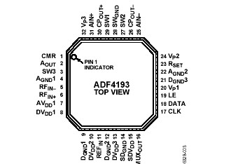
ADF4193: Features: New, fast settling, fractional-N PLL architecture Single PLL replaces ping-pong synthesizers Frequency hop across GSM band in 5 s with phase settled by 20 s 0.5 degree rms phase error at ...

floor Price/Ceiling Price

Part Number:
ADF4193
Supply Ability:
5000

Price Break

  • Qty
  • 1~5000
  • Unit Price
  • Negotiable
  • Processing time
  • 15 Days
Total Cost: $ 0.00

SeekIC Buyer Protection PLUS - newly updated for 2013!

  • Escrow Protection.
  • Guaranteed refunds.
  • Secure payments.
  • Learn more >>

Month Sales

268 Transactions

Rating

evaluate  (4.8 stars)

Upload time: 2024/4/30

Payment Methods

All payment methods are secure and covered by SeekIC Buyer Protection PLUS.

Notice: When you place an order, your payment is made to SeekIC and not to your seller. SeekIC only pays the seller after confirming you have received your order. We will also never share your payment details with your seller.
Product Details

Description


Features:

New, fast settling, fractional-N PLL architecture
Single PLL replaces ping-pong synthesizers
Frequency hop across GSM band in 5 s with phase settled by 20 s
0.5 degree rms phase error at 2 GHz RF output
Digitally programmable output phase
RF input range up to 3.5 GHz
3-wire serial interface
On-chip, low noise differential amplifier
Phase noise figure of merit: 216 dBc/Hz
Loop filter design possible using ADI SimPLL


Application

GSM/EDGE base stations
PHS base stations
Instrumentation and test equipment


Pinout

  Connection Diagram


Specifications

Parameter Rating
AVDD to GND
AVDD to DVDD, SDVDD
VP to GND
VP to AVDD
Digital I/O Voltage to GND
Analog I/O Voltage to GND
REFIN, RFIN+, RFIN to GND
Operating Temperature Range  
   Industrial (B Version)
Storage Temperature Range
Maximum Junction Temperature
LFCSP JA Thermal Impedance
    (Paddle-Soldered)
Reflow Soldering
   Peak Temperature
   Time at Peak Temperature
0.3 V to +3.6 V
0.3 V to +0.3 V
0.3 V to +5.8 V
0.3 V to +5.8 V
0.3 V to VDD + 0.3 V
0.3 V to VP + 0.3 V
0.3 V to VDD + 0.3 V

40°C to +85°C
65°C to +125°C
150°C
27.3°C/W

260°C
40 sec


Description

The ADF4193 frequency synthesizer can be used to implement local oscillators in the upconversion and downconversion sections of wireless receivers and transmitters. Its architecture is specifically designed to meet the GSM/EDGE lock time requirements for base stations. ADF4193 consists of a low noise, digital phase frequency detector (PFD), and a precision differential charge pump. There is also a differential amplifier to convert the differential charge pump output to a single-ended voltage for the external voltage controlled oscillator (VCO).

The - based fractional interpolator, working with the N divider, allow programmable modulus fractional-N division. Additionally, the 4-bit reference (R) counter and on-chip frequency doubler allow selectable reference signal (REFIN) frequencies at the PFD input. A complete phase-locked loop (PLL) can be implemented if the synthesizer is used with an external loop filter and a VCO. The switching architecture of ADF4193 ensures that the PLL settles inside the GSM time slot guard period, removing the need for a second PLL and associated isolation switches. This decreases cost, complexity, PCB area, shielding, and characterization on previous ping-pong GSM PLL architectures.


Customers Who Bought This Item Also Bought

Margin,quality,low-cost products with low minimum orders. Secure your online payments with SeekIC Buyer Protection.
Tapes, Adhesives
803
Isolators
Boxes, Enclosures, Racks
Test Equipment
Cables, Wires
View more