Features: 44 V Supply Maximum Ratings
VSS to VDD Analog Signal Range
Low On Resistance (60 V typ)
Low Power Consumption (1.6 mW max)
Low Charge Injection (<4 pC typ)
Fast Switching
Break-Before-Make Switching Action
Plug-In Replacement for DG428/DG429ApplicationAutomatic Test Equipment
Data Acquisition Systems
Communication Systems
Avionics and Military Systems
Microprocessor Controlled Analog Systems
Medical InstrumentationPinout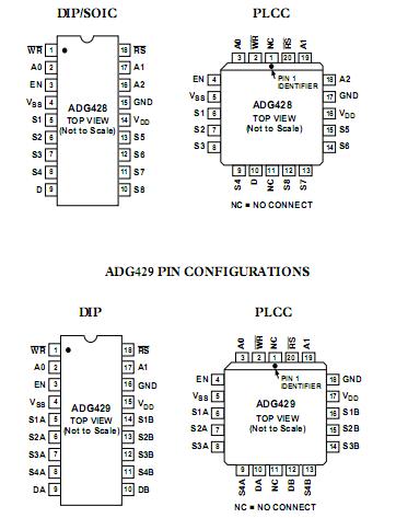 SpecificationsVDD to VSS . . . . . . . . . . . . . . . . . . . . . . . . . . . . . . . . . ..+44 V
VDD to GND . . . . . . . . . . . . . . . . . . . . . . . . . . 0.3 V to +25 V
VSS to GND . . . . . . . . . . . . . . . . . . . . . . . . . . +0.3 V to 25 V
Analog, Digital Inputs2 . . . . . . . . . . VSS 2 V to VDD + 2 V or
30 mA, Whichever Occurs First
Continuous Current, S or D . . . . . . . . . . . . . . . . . . . . . 30 mA
Peak Current, S or D . . . . . . . . . . . . . . . . . . . . . . . . . .100 mA
(Pulsed at 1 ms, 10% Duty Cycle Max)
Operating Temperature Range
Industrial (B Version) . . . . . . . . . . . . . . . . . 40°C to +85°C
Extended (T Version) . . . . . . . . . . . . . . . . 55°C to +125°C
Storage Temperature Range . . . . . . . . . . .65°C to +150°C
Junction Temperature . . . . . . . . . . . . . . . . . . . . . . . .+150°C
Cerdip Package, Power Dissipation . . . . . . . . . . . . 900 mW
JA, Thermal Impedance . . . . . . . . . . . . . . . . . . . . . 73°C/W
Lead Temperature, Soldering (10 sec) . . . . . . . . . . +300°C
Plastic Package, Power Dissipation . . . . . . . . . . . . 470 mW
JA, Thermal Impedance . . . . . . . . . . . . . . . . . . . .115°C/W
Lead Temperature, Soldering (10 sec) . . . . . . . . . . +260°C
SOIC Package, Power Dissipation . . . . . . . . . . . . . .600 mW
JA, Thermal Impedance . . . . . . . . . . . . . . . . . . . . .77°C/WDescriptionThe ADG428/ADG429 are monolithic CMOS analog multiplexers comprising eight single channels and four differential channels respectively. On-chip address and control latches facilitate microprocessor interfacing. The ADG428 switches one of eight inputs to a common output as determined by the 3-bit binary address lines A0, A1 and A2. The ADG428/ADG429 switches one of four differential inputs to a common differential output as determined by the 2-bit binary address lines A0 and A1. An EN input on both devices is used to enable or disable the ADG428/ADG429. When disabled, all channels are switched OFF. All the control
inputs, address and enable inputs are TTL compatible over the full specified operating temperature range. This makes the part suitable for bus-controlled systems such as data acquisition systems, process controls, avionics and ATEs because the TTL-compatible address latches simplify the digital interface design and reduce the board space required.
The ADG428/ADG429 are designed on an enhanced LC
2MOS process that provides low power dissipation yet gives high switching speed and low on resistance. Each channel conducts equally well in both directions when ON and has an input signal range that extends to the supplies. In the OFF condition, signal levels up to the supplies are blocked. All channels exhibit break-before-make switching action, preventing momentary shorting when switching
channels. Inherent in the design is low charge injection for minimum transients when switching the digital inputs. The ADG428/ADG429 are improved replacements for the DG428/DG429 Analog Multiplexers.

 ADG428 Data Sheet