Features: `+5 V, 65 V Power Supplies
`Ultralow Power Dissipation (<0.5 W)
`Low Leakage (<100 pA)
`Low On Resistance (<50 )
`Fast Switching Times
`Low Charge Injection
`TTL/CMOS Compatible
`TSSOP PackageApplication·Battery Powered Instruments
·Single Supply Systems
·Remote Powered Equipment
·+5 V Supply Systems
·Computer Peripherals such as Disk Drives
·Precision Instrumentation
·Audio and Video Switching
·Automatic Test Equipment
·Precision Data Acquisition
·Sample Hold Systems
·Communication SystemsPinout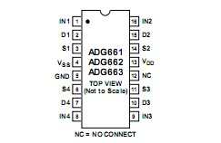 Specifications
(TA = +25 unless otherwise noted)
VDD to VSS .........................................................+44 V
VDD to GND ........................................0.3 V to +25 V
VSS to GND ........................................ +0.3 V to 25 V
Analog, Digital Inputs2 ......... VSS 2 V to VDD +2 V or
30 mA, Whichever Occurs First
Continuous Current, S or D ...............................30 mA
Peak Current, S or D ........................................100 mA
(Pulsed at 1 ms, 10% Duty Cycle max)
Operating Temperature Range
Industrial (B Version) .......................... 40 to +85
Storage Temperature Range ..................65 to +150
Junction Temperature .........................................+150
TSSOP Package, Power Dissipation....................450 mW
JA Thermal Impedance.................................... 115/W
JC Thermal Impedance ......................................35/W
Lead Temperature, Soldering
Vapor Phase (60 secs)......................................... +215
Infrared (15 secs).................................................+220
NOTES
1Stresses above those listed under Absolute Maximum Ratings may cause perma- nent damage to the device. This is a stress rating only; functional operation of the device at these or any other conditions above those listed in the operational sections of this specification is not implied. Exposure to absolute maximum rating conditions for extended periods may affect device reliability. Only one absolute maximum rating may be applied at any one time.
2Overvoltages at IN, S or D will be clamped by internal diodes. Current should be
limited to the maximum ratings given.
DescriptionThe ADG661, ADG662 and ADG663 are monolithic CMOS devices comprising four independently selectable switches. These switches feature low, well-controlled on resistance and wide analog signal range, making them ideal for precision analog
signal switching.
They are fabricated using Analog Devices' advanced linear compatible CMOS (LC2
MOS) process, which offers benefits of low leakage currents, ultralow power dissipation and low capaci tance for fast switching speeds with minimum charge injection. The on resistance profile is very flat over the full analog input range ensuring excellent linearity and low distortion when switching audio signals. Fast switching speed coupled with high signal bandwidth also make the ADG661, ADG662 and ADG663 be suitable for video signal switching. CMOS construction ensures ultralow power dissipa-
tion making the parts ideally suited for portable and battery powered instruments.
The ADG661, ADG662 and ADG663 contain four indepen- dent SPST switches. The ADG661, ADG662 and ADG663 differ only in that the digital control logic is inverted. The ADG661 switches are turned on with a logic low on the appropriate control input,
while a logic high is required for the ADG662. The ADG663 has two switches with digital control logic similar to that of the ADG661, while the logic is inverted on the other two switches.
Each switch conducts equally well in both directions when ON and has an input signal range that extends to the supplies. In the OFF condition, signal levels up to the supplies are blocked. All switches of ADG661, ADG662 and ADG663 exhibit break-before-make switching action for use in multiplexer applications. Inherent in the design is low charge injection for minimum transients when switching the digital inputs.

 ADG663 Data Sheet