Features: ADVANCED CMOS EEPROM TECHNOLOGY
LOW VCC OPERATION ¼ Vcc = 0.9V ~ 3.6V
AK93C41A ` ` 1024 bits, 64 ´ 16 organization
AK93C51A ` ` 2048 bits, 128 ´ 16 organization
SERIAL INTERFACE
- Interfaces with popular microcontrollers and standard microprocessors
LOW POWER CONSUMPTION
- 10mA Max. Standby (VCC=3.6V)
Automatic address increment (READ)
Automatic write cycle time-out with auto-ERASE
Busy/Ready status signal
Software controlled write protection
Hardware write protect for lower block (AK93C51A only)
IDEAL FOR LOW DENSITY DATA STORAGE
- Low cost, space saving, 8-pin package
Pinout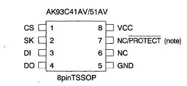 Specifications
|
Parameter |
Symbol |
Min |
Max |
Unit |
|
Power Supply |
VCC |
-0.6 |
+5.0 |
V |
|
All Input Voltages
with Respect to Ground |
VIO
|
-0.6
|
VCC+0.6
|
V
|
|
Ambient storage temperature |
Tst |
-65 |
+150 |
°C |
DescriptionThe AK93C41A/51A is a 1024/2048-bit serial CMOS EEPROM divided into 64/128 registers of 16 bits each.The AK93C41A/51A has 4 instructions such as READ, WRITE, EWEN and EWDS. Those instructions control the AK93C41A/51A.The AK93C41A/51A can operate full function under wide operating voltage range from 0.9V to 3.6V. The charge up circuit is integrated for high voltage generation that is used for write operation.A serial interface of AK93C41A/51A, consisting of chip select (CS), serial clock (SK), data-in (DI) and dataout (DO), can easily be controlled by popular microcontrollers or standard microprocessors. AK93C41A/51A takes in the write data from data input pin (DI) to a register synchronously with rising edge of input pulse of serial clock pin (SK). And at read operation, AK93C41A/51A takes out the read data from a register to data output pin (DO) synchronously with rising edge of SK.The DO pin is usually in high impedance state. The DO pin outputs "L" or "H" in case of data output or Busy/Ready signal output.Software and Hardware controlled write protection When Vcc is applied to the part, the part automatically powers up in the ERASE/WRITE Disable state. In the ERASE/WRITE disable state, execution of WRITE instruction is disabled. Before WRITE instruction is executed, EWEN instruction must be executed. The ERASE/WRITE enable state continues until EWDS instruction is executed or Vcc is removed from the part.Execution of a read instruction is independent of both EWEN and EWDS instructions.
The PROTECT pin is available only on the AK93C41A/51A. When PROTECT pin is tied to GND, PROGRAM operations onto the lower 1Kbit ($00a$3F) will not be executed. When PROTECT pin is tied to VCC, normal operation is enabled. There is an internal pull-down on the PROTECT pin.Busy/Ready status signal After a write instruction, the DO output serves as a Busy/Ready status indicator. After the falling edge of the CS initiates the self-timed programming cycle, the DO indicates the Busy/Ready status of the chip if the CS is brought high after a minimum of 250ns (Tcs). DO=logical "0" indicates that programming is still in progress.DO=logical "1" indicates that the register at the address specified in the instruction has been written with the new data pattern contained in the instruction and the part is ready for a next instruction.The Busy/Ready status indicator is only valid when CS is active (high). When CS is low, the DO output goes into a high impedance state.The Busy/Ready signal outputs until a start bit (Logic"1") of the next instruction is given to the part.

 AK93C51A Data Sheet


