Features: • Programmable Audio Output for Interfacing with Common Audio DAC
PCM Format Compatible
I2S Format Compatible
• 8-bit MCU C51 Core-based (FMAX = 20 MHz)
• 2304 Bytes of Internal RAM
• 64K Bytes of Code Memory
AT89C5132: Flash (100K Write/Erase Cycles)
• 4K Bytes of Boot Flash Memory (AT89C5132)
ISP: Download from USB or UART to any External Memory Cards
• USB Rev 1.1 Device Controller
"Full Speed" Data Transmission
• Built-in PLL
• MultiMedia Card® Interface Compatibility
• Atmel DataFlash® SPI Interface Compatibility
• IDE/ATAPI Interface
• 2 Channels 10-bit ADC, 8 kHz (8 True Bits)
Battery Voltage Monitoring
Voice Recording Controlled by Software
• Up to 44 Bits of General-purpose I/Os
4-bit Interrupt Keyboard Port for a 4 x n Matrix
SmartMedia® Software Interface
• Two Standard 16-bit Timers/Counters
• Hardware Watchdog Timer
• Standard Full Duplex UART with Baud Rate Generator
• Two Wire Master and Slave Modes Controller
• SPI Master and Slave Modes Controller
• Power Management
Power-on Reset
Software Programmable MCU Clock
Idle Mode, Power-down Mode
• Operating Conditions
3V, ±10%, 25 mA Typical Operating at 25°C
Temperature Range: -40°C to +85°C
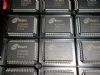
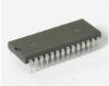
• Packages
TQFP80, PLCC84 (Development Board Only)
Dice
Application• Flash Recorder/Writer
• PDA, Camera, Mobile Phone
• PC Add-onPinout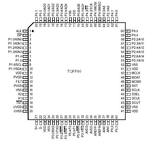 Specifications
|
Storage Temperature ................................... -65°C to +150°C
Voltage on any other Pin to VSS ............................-0.3 to +4.0V
IOL per I/O Pin ................................................................... 5 mA
Power Dissipation................................................................. 1 W
Ambient Temperature Under Bias..................... -40°C to +85°C
VDD .......................................................................... 2.7V to 3.3V
|
DescriptionThe AT89C5132 is a mass storage device controlling data exchange between various Flash modules, HDD and CD-ROM.
The AT89C5132 includes 64K Bytes of Flash memory and allows In-System Programming through an embedded 4K Bytes of Boot Flash Memory.
The AT89C5132 include 2304 Bytes of RAM memory.
The AT89C5132 provides all the necessary features for man-machine interface including, timers, keyboard port, serial or parallel interface (USB, SPI, IDE), ADC input, I2S output, and all external memory interface (NAND or NOR Flash, SmartMedia, MultiMedia, DataFlash cards).

 AT89C5132 Data Sheet