Features: • Ultra low operation voltage : 1.8 ~ 3.6V
• Ultra low power consumption :
Vcc = 2.0 V C-grade: 15mA (Max.) operating current
I-grade: 20mA (Max.) operating current
0.08uA (Typ.) CMOS standby current
Vcc = 3.0 V C-grade: 20mA (Max.) operating current
I -grade: 25mA (Max.) operating current
0.1uA (Typ.) CMOS standby current
• High speed access time :
-70 70ns (Max.) at Vcc = 2.0V
-10 100ns (Max.) at Vcc = 2.0V
• Automatic power down when chip is deselected
• Three state outputs and TTL compatible
• Fully static operation
• Data retention supply voltage as low as 1.5V
• Easy expansion with CE and OE options
• I/O Configuration x8/x16 selectable by LB and UB pinPinout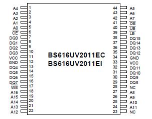 Specifications
| SYMBOL |
PARAMETER |
RATING |
UNITS |
| VTERM |
Terminal Voltage with Respect to GND |
-0.5 to Vcc+0.5 |
V |
| TBIAS |
Temperature Under Bias |
-40 to +125 |
|
| TSTG |
Storage Temperature |
-60 to +150 |
|
| PT |
Power Dissipation |
1.0 |
W |
| IOUT |
DC Output Current |
20 |
mA |
1. Stresses greater than those listed under ABSOLUTE MAXIMUM RATINGS may cause permanent damage to the device. This is a stress rating only and functional operation of the device at these or any other conditions above those indicated in the operational sections of this specification is not implied. Exposure to absolute maximum rating conditions for extended periods may affect reliability.DescriptionThe BS616UV2011 is a high performance, Ultra low power CMOS Static Random Access Memory organized as 131,072 words by 16 bits and operates from a wide range of 1.8V to 3.6V supply voltage.
Advanced CMOS technology and circuit techniques of BS616UV2011EC provide both high speed and low power features with a typical CMOS standby current of 0.08uA and maximum access time of 70/100ns in 2.0V operation.
Easy memory expansion of BS616UV2011EC is provided by an active LOW chip enable(CE), active LOW output enable(OE) and three-state output drivers.
The BS616UV2011 has an automatic power down feature, reducing the power consumption significantly when chip is deselected.
The BS616UV2011 is available in DICE form, JEDEC standard 44-pin TSOP Type II package , JEDEC standard 48-pin TSOP Type I package and 48-ball BGA package.

 BS616UV2011EC Data Sheet