Crosstalk
:
Bandwidth
:
Number of Switches
:
Switch Configuration
:
Switch Voltage (Max)
:
Mounting Style
: SMD/SMT
Maximum Operating Temperature
: + 105 C
On Resistance (Max)
: 0.09 Ohms
On Time (Max)
: 55 us
Off Time (Max)
: 95 us
Operating Supply Voltage
: 7 V to 58 V
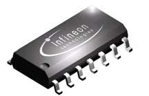
Package / Case
: DSO-14
Application• µC compatible high-side power switch with diagnostic feedback for 12V and 24V and42V grounded loads
• All types of resistive, inductive and capacitive loads
• Most suitable for inductive loads
• Replaces electromechanical relays, fuses and discrete circuitsPinout Specifications
| Parameter |
Symbol |
Values |
Unit |
| Supply voltage (overvoltage protection see page 6) |
Vbb |
58 |
V |
Supply voltage for full short circuit protection
Tj,start =-40 ...+150°C |
Vbb |
50 |
V |
| Output Voltage to Vbb |
VON |
70 |
V |
| Negative voltage slope at output |
-dVOUT/dt |
20 |
V/s |
| Load current (Short-circuit current, see page 7) |
IL |
IL(LIM)1) |
A |
Load dump protection2) VLoadDump = VA + Vs, VA = 27 V
RI3)= 8,td= 200 ms, IN= low or high
each channel loaded with RL = 20, |
VLoaddump4) |
70 |
V |
Operating temperature range
Storage temperature range |
Tj
Tstg |
-40 ...+150
-55 ...+150 |
°C |
Power dissipation (DC)5) Ta = 25°C:
(all channels active) Ta = 85°C: |
Ptot |
3.0
1.6 |
W |
Maximal switchable inductance, single pulse
Vbb =12V, Tj,start =150°C5),
IL = 2.5A, EAS = 110 mJ, 0 one channel:
IL = 3.5A, EAS = 278 mJ, 0 two parallel channels: |
ZL |
23.0
30.0 |
mH |
Electrostatic discharge capability (ESD)
(Human Body Model)acc. MIL-STD883D, method 3015.7 and ESD assn. std. S5.1-1993 R=1.5k; C=100pF |
VESD |
1.0
|
kV |
| Input voltage (DC) |
VIN |
±42 |
V |
Current through input pin (DC)
Current through status pin (DC) |
IIN
IST |
±2.0
±2.0 |
mA |
| Status pull up voltage |
VSPU
|
±42 |
V
|
DescriptionThe BTS723GW is designed as one kind of smart high-side power switch. The general description of this device are:(1)N channel vertical power MOSFET with charge pump, ground referenced CMOS compatible input and diagnostic feedback, monolithically integrated in Smart SIPMOS 80V technology.; (3)Providing embedded protective functions; (4)An array of resistors is integrated in order to reduce the external components.
The BTS723GW can be used in (1)uC compatible high-side power switch with diagnostic feedback for 12V and 24V and 42V grounded loads; (2)all types of resistive, inductive and capacitive loads; (3)most suitable for inductive loads; (4)replaces electromechanical relays, fuses and discrete circuits. And the basic functions of it are:(1)CMOS compatible input; (2)improved electromagnetic compatibility (EMC); (3)fast demagnetization of inductive loads; (4)stable behaviour at undervoltage; (5)wide operating voltage range; (6)logic ground independent from load ground; (7)optimized inverscurrent capability.
The absolute maximum ratings of the BTS723GW can be summarized as:(1)supply voltage:58 V;(2)supply voltage for full short circuit protection:50 V;(3)output voltage to Vbb:70 V;(4)negative voltage slope at output:20 V/s;(5)load current:IL(LIM) A;(6)operating temperature range:-40 to +150;(7)storage temperature range:-55 to +150;(8)power dissipation (DC):3.0 W;(9)status pull up voltage:±42 V. If you want to know more information such as the electrical characteristics about the BTS723GW, please download the datasheet in www.seekic.com or www.chinaicmart.com .
The BTS723GW features are as follows:
• N channel vertical power MOSFET with charge pump, ground referenced CMOS compatible input and diagnostic feedback, monolithically integrated in Smart SIPMOS
® 80V technology.
• Providing embedded protective functions
• An array of resistors is integrated in order to reduce the external components
Parameters: | Technical/Catalog Information | BTS723GW |
| Vendor | Infineon Technologies |
| Category | Integrated Circuits (ICs) |
| Package / Case | DSO-14 |
| Mounting Type | Surface Mount |
| Type | High Side |
| Voltage - Supply | 7 V ~ 58 V |
| On-State Resistance | 90 mOhm |
| Current - Output / Channel | 2.9A |
| Current - Peak Output | 9A |
| Packaging | Tape & Reel (TR) |
| Input Type | Non-Inverting |
| Number of Outputs | 2 |
| Operating Temperature | -40°C ~ 150°C |
| Lead Free Status | Lead Free |
| RoHS Status | RoHS Compliant |
| Other Names | BTS723GW
BTS723GW
|
 BTS723GW Data Sheet