C161S

Application• High Performance 16-bit CPU with 4-Stage Pipeline 80 ns Instruction Cycle Time at 25 MHz CPU Clock 400 ns Multiplication (16 * 16 bit), 800 ns Division (32 / 16 bit) Enhanced Boolean Bit Manipulation Facilities Additional Instructions to Support HLL and Operating Systems Registe...

product image

C161S Picture
SeekIC No. : 004308034 Detail

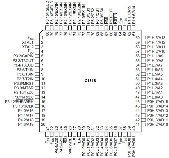
C161S: Application• High Performance 16-bit CPU with 4-Stage Pipeline 80 ns Instruction Cycle Time at 25 MHz CPU Clock 400 ns Multiplication (16 * 16 bit), 800 ns Division (32 / 16 bit) Enhanced Bool...

floor Price/Ceiling Price

Part Number:
C161S
Supply Ability:
5000

Price Break

  • Qty
  • 1~5000
  • Unit Price
  • Negotiable
  • Processing time
  • 15 Days
Total Cost: $ 0.00

SeekIC Buyer Protection PLUS - newly updated for 2013!

  • Escrow Protection.
  • Guaranteed refunds.
  • Secure payments.
  • Learn more >>

Month Sales

268 Transactions

Rating

evaluate  (4.8 stars)

Upload time: 2024/4/25

Payment Methods

All payment methods are secure and covered by SeekIC Buyer Protection PLUS.

Notice: When you place an order, your payment is made to SeekIC and not to your seller. SeekIC only pays the seller after confirming you have received your order. We will also never share your payment details with your seller.
Product Details

Description


Application

• High Performance 16-bit CPU with 4-Stage Pipeline
80 ns Instruction Cycle Time at 25 MHz CPU Clock
400 ns Multiplication (16 * 16 bit), 800 ns Division (32 / 16 bit)
Enhanced Boolean Bit Manipulation Facilities
Additional Instructions to Support HLL and Operating Systems
Register-Based Design with Multiple Variable Register Banks
Single-Cycle Context Switching Support
16 Mbytes Total Linear Address Space for Code and Data
1024 Bytes On-Chip Special Function Register Area
• 16-Priority-Level Interrupt System with 30 Sources, Sample-Rate down to 40 ns
• 8-Channel Interrupt-Driven Single-Cycle Data Transfer Facilities via Peripheral Event Controller (PEC)
• Clock Generation via on-chip PLL (factors 1:1.5/2/2.5/3/4/5), via prescaler or via direct clock input
• On-Chip Memory Modules: 2 Kbytes On-Chip Internal RAM (IRAM)
• On-Chip Peripheral Modules
Two Multi-Functional General Purpose Timer Units with 5 Timers
Two Serial Channels (Sync./Asynchronous and High-Speed-Synchronous)
On-Chip Real Time Clock
• External Address Space for Code and Data
Programmable External Bus Characteristics for Different Address Ranges
Multiplexed or Demultiplexed External Address/Data Buses with 8-bit or 16-bit Data Bus Width
Four Programmable Chip-Select Signals
4 Mbytes maximum address window size, results in a total external address space of 16 Mbytes, when all chip-select signal (address windows) are active
• Idle and Power Down Modes with Flexible Power Management
• Programmable Watchdog Timer and Oscillator Watchdog
• Up to 63 General Purpose I/O Lines, partly with Selectable Input Thresholds and Hysteresis
• Power Supply: the C161S can operate from a 5 V or a 3 V power supply (see Table 1)
• Supported by a Large Range of Development Tools like C-Compilers, Macro-Assembler Packages, Emulators, Evaluation Boards, HLL-Debuggers, Simulators, Logic Analyzer Disassemblers, Programming Boards
• On-Chip Bootstrap Loader
• 80-Pin MQFP Package


Pinout

  Connection Diagram


Specifications

Parameter
Symbol
Limit Values
Unit
Notes
Min.
Max.
Storage temperature
TST
-65
150
-
Junction temperature
TJ
-40
150
under bias
Voltage on VDD pins with
respect to ground (VSS)
VDD
-0.5
6.5
V
-
Voltage on any pin with
respect to ground (VSS)
VIN
-0.5
VDD + 0.5
V
-
Input current on any pin
during overload condition
IOV
-10
10
mA
-
Absolute sum of all input
currents during overload
condition
|IOV|
-
100
mA
-
Power dissipation
PDISS
-
1.5
W
-
Note: Stresses above those listed under "Absolute Maximum Ratings" may cause permanent damage to the device. This is a stress rating only and functional operation of the device at these or any other conditions above those indicated in the operational sections of this specification is not implied. Exposure to absolute  maximum rating conditions for extended periods may affect device reliability. During absolute maximum rating overload conditions (VIN > VDD or VIN < VSS) the voltage on VDD pins with respect to ground (VSS) must not exceed the values defined by the absolute maximum ratings.


Description

The architecture of the C161S combines advantages of both RISC and CISC processors and of advanced peripheral subsystems in a very well-balanced way. In addition the onchip memory blocks allow the design of compact systems with maximum performance. Figure 3 gives an overview of the different on-chip components and of the advanced, high bandwidth internal bus structure of the C161S.


Customers Who Bought This Item Also Bought

Margin,quality,low-cost products with low minimum orders. Secure your online payments with SeekIC Buyer Protection.
Inductors, Coils, Chokes
Programmers, Development Systems
Motors, Solenoids, Driver Boards/Modules
Semiconductor Modules
Soldering, Desoldering, Rework Products
View more