CD40175BMS

Features: • High Voltage Type (20V Rating)• Output Compatible with Two HTL Loads, Two Low Power TTL Loads, or One Low Power Schottky TTL Load• Functional Equivalent to TTL74175• 100% Tested for Quiescent Current at 20V• 5V, 10V and 15V Parametric Ratings• Maximu...

product image

CD40175BMS Picture
SeekIC No. : 004311205 Detail

CD40175BMS: Features: • High Voltage Type (20V Rating)• Output Compatible with Two HTL Loads, Two Low Power TTL Loads, or One Low Power Schottky TTL Load• Functional Equivalent to TTL74175R...

floor Price/Ceiling Price

Part Number:
CD40175BMS
Supply Ability:
5000

Price Break

  • Qty
  • 1~5000
  • Unit Price
  • Negotiable
  • Processing time
  • 15 Days
Total Cost: $ 0.00

SeekIC Buyer Protection PLUS - newly updated for 2013!

  • Escrow Protection.
  • Guaranteed refunds.
  • Secure payments.
  • Learn more >>

Month Sales

268 Transactions

Rating

evaluate  (4.8 stars)

Upload time: 2024/4/29

Payment Methods

All payment methods are secure and covered by SeekIC Buyer Protection PLUS.

Notice: When you place an order, your payment is made to SeekIC and not to your seller. SeekIC only pays the seller after confirming you have received your order. We will also never share your payment details with your seller.
Product Details

Description


Features:

• High Voltage Type (20V Rating)
• Output Compatible with Two HTL Loads, Two Low Power
   TTL Loads, or One Low Power Schottky TTL Load
• Functional Equivalent to TTL74175
• 100% Tested for Quiescent Current at 20V
• 5V, 10V and 15V Parametric Ratings
• Maximum Input Current of 1A at 18V Over Full Package
   Temperature Range; 100nA at 18V and +25
• Noise Margin (Over Full Package/Temperature Range)
   - 1V at VDD = 5V
   - 2V at VDD = 10V
   - 2.5V at VDD = 15V
• Standardized Symmetrical Output Characteristics
• Meets All Requirements of JEDEC Tentative Standard No. 13B, "Standard Specifications for Description of 'B' Series CMOS Devices"


Application

• Shift Registers
• Buffer/Storage Registers
• Pattern Generators


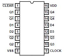
Pinout

  Connection Diagram


Specifications

DC Supply Voltage Range, (VDD) . . . . . . . . . . . . . . . -0.5V to +20V
(Voltage Referenced to VSS Terminals)
Input Voltage Range, All Inputs . . . . . . . . . . . . .-0.5V to VDD +0.5V
DC Input Current, Any One Input . . . . . . . . . . . . . . . . . . . . .±10mA
Operating Temperature Range. . . . . . . . . . . . . . . . -55  to +125
Package Types D, F, K, H
Storage Temperature Range (TSTG) . . . . . . . . . . . ..-65  to +150
Lead Temperature (During Soldering) . . . . . . . . . . . . ... . . . . +265
At Distance 1/16 ± 1/32 Inch (1.59mm ± 0.79mm) from case for 10s Maximum


Description

CD40175BMS consists of four identical D-type flip-flops. Each flip-flop has an independent DATA D input and complementary Q and Q outputs. The CLOCK and CLEAR inputs are common to all flip-flops. Data are transferred to the Q  outputs on the positive going transition of the clock pulse. All four flip-flops are simultaneously reset by a low level on the CLEAR input.

CD40175BMS can function as shift register elements or as T-type flip-flops for toggle and counter applications.

The CD40175BMS is supplied in these 16-lead outline packages:
Braze Seal DIP                 H4T
Ceramic Flatpack              H6W


Customers Who Bought This Item Also Bought

Margin,quality,low-cost products with low minimum orders. Secure your online payments with SeekIC Buyer Protection.
RF and RFID
Memory Cards, Modules
Programmers, Development Systems
Optical Inspection Equipment
Power Supplies - Board Mount
View more