CD4027BC

Features: Wide supply voltage range 3.0V to 15V High noise immunity 0.45 VDD (typ.) Low power TTL Fan out of 2 driving 74L compatibility or 1 driving 74LS Low power 50 nW (typ.) Medium speed operation+ 12 MHz (typ.) with 10V supplyPinoutSpecificationsIf Military/Aerospace specified devices are re...

product image

CD4027BC Picture
SeekIC No. : 004311246 Detail

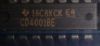
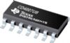
CD4027BC: Features: Wide supply voltage range 3.0V to 15V High noise immunity 0.45 VDD (typ.) Low power TTL Fan out of 2 driving 74L compatibility or 1 driving 74LS Low power 50 nW (typ.) Medium speed operat...

floor Price/Ceiling Price

Part Number:
CD4027BC
Supply Ability:
5000

Price Break

  • Qty
  • 1~5000
  • Unit Price
  • Negotiable
  • Processing time
  • 15 Days
Total Cost: $ 0.00

SeekIC Buyer Protection PLUS - newly updated for 2013!

  • Escrow Protection.
  • Guaranteed refunds.
  • Secure payments.
  • Learn more >>

Month Sales

268 Transactions

Rating

evaluate  (4.8 stars)

Upload time: 2024/4/29

Payment Methods

All payment methods are secure and covered by SeekIC Buyer Protection PLUS.

Notice: When you place an order, your payment is made to SeekIC and not to your seller. SeekIC only pays the seller after confirming you have received your order. We will also never share your payment details with your seller.
Product Details

Description


Features:

Wide supply voltage range 3.0V to 15V
High noise immunity 0.45 VDD (typ.)
Low power TTL Fan out of 2 driving 74L compatibility or 1 driving 74LS
Low power 50 nW (typ.)
Medium speed operation+ 12 MHz (typ.)
                                with 10V supply


Pinout

  Connection Diagram


Specifications

If Military/Aerospace specified devices are required, please contact the National Semiconductor Sales Office/Distributors for availability and specifications.
DC Supply Voltage (VDD)  . . . . . . . . . . . . . .b0.5 VDC to a18 VDC
Input Voltage (VIN) . . . . . . . . . .  . . .. . . . b0.5V to VDD a0.5 VDC
Storage Temperature Range (TS)  . . . . . . . . . . .b65ßC to a150ßC
Power Dissipation (PD)
 Dual-In-Line  . . . . . . . . . . . . . . . . . . . . . . . . . . . . . . . . . .700 mW
 Small Outline  . . . . . . . . . . . . . . . . . . . . . . . . . . . . . . . . . .500 mW
Lead Temperature (TL)
 (Soldering, 10 seconds)  . . . . . . . . . . . . . . . . . . . . . . . . . . .260ßC


Description

CD4027BC dual J-K flip-flops are monolithic complementary MOS (CMOS) integrated circuits constructed with N- and Pchannel enhancement mode transistors. Each flip-flop has independent J, K, set, reset, and clock inputs and buffered
Q and Q outputs. These CD4027BC flip-flops are edge sensitive to the clock input and change state on the positive-going transition of the clock pulses. Set or reset is independent of the clock and is accomplished by a high level on the respective input. All CD4027BC inputs are protected against damage due to static discharge by diode clamps to VDD and VSS.


Customers Who Bought This Item Also Bought

Margin,quality,low-cost products with low minimum orders. Secure your online payments with SeekIC Buyer Protection.
Programmers, Development Systems
Line Protection, Backups
Circuit Protection
Connectors, Interconnects
View more