SeekIC No. : 004311270
Detail
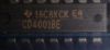
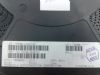
CD4041BMS: DescriptionThe CD4041BMS is designed as one kind of CMOS quad true / complement buffer that can be used in (1)High Current Source/Sink Driver; (2)CMOS-to-DTL/TTL Converter Buffer; (3)Display Driver;...
 CD4041BMS Data Sheet
floor Price/Ceiling Price
- Part Number:
- CD4041BMS
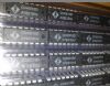
- Supply Ability:
- 5000
Price Break
- Qty
- 1~5000
- Unit Price
- Negotiable
- Processing time
- 15 Days
SeekIC Buyer Protection PLUS - newly updated for 2013!
- Escrow Protection.
- Guaranteed refunds.
- Secure payments.
- Learn more >>
Month Sales
268 Transactions
Payment Methods
All payment methods are secure and covered by SeekIC Buyer Protection PLUS.
Notice: When you place an order, your payment is made to SeekIC and not to your seller. SeekIC only pays the seller after confirming you have received your order. We will also never share your payment details with your seller.