CD4043BMS

Features: * High Voltage Types (20V Rating)* Quad NOR R/S Latch- CD4043BMS* Quad NAND R/S Latch - CD4044BMS* 3 State Outputs with Common Output ENABLE* Separate SET and RESET Inputs for Each Latch* NOR and NAND Configuration* 5V, 10V and 15V Parametric Ratings* Standardized Symmetrical Output Char...

product image

CD4043BMS Picture
SeekIC No. : 004311280 Detail

CD4043BMS: Features: * High Voltage Types (20V Rating)* Quad NOR R/S Latch- CD4043BMS* Quad NAND R/S Latch - CD4044BMS* 3 State Outputs with Common Output ENABLE* Separate SET and RESET Inputs for Each Latch* ...

floor Price/Ceiling Price

Part Number:
CD4043BMS
Supply Ability:
5000

Price Break

  • Qty
  • 1~5000
  • Unit Price
  • Negotiable
  • Processing time
  • 15 Days
Total Cost: $ 0.00

SeekIC Buyer Protection PLUS - newly updated for 2013!

  • Escrow Protection.
  • Guaranteed refunds.
  • Secure payments.
  • Learn more >>

Month Sales

268 Transactions

Rating

evaluate  (4.8 stars)

Upload time: 2024/4/17

Payment Methods

All payment methods are secure and covered by SeekIC Buyer Protection PLUS.

Notice: When you place an order, your payment is made to SeekIC and not to your seller. SeekIC only pays the seller after confirming you have received your order. We will also never share your payment details with your seller.
Product Details

Description


Features:

* High Voltage Types (20V Rating)
* Quad NOR R/S Latch- CD4043BMS
* Quad NAND R/S Latch - CD4044BMS
* 3 State Outputs with Common Output ENABLE
* Separate SET and RESET Inputs for Each Latch
* NOR and NAND Configuration
* 5V, 10V and 15V Parametric Ratings
* Standardized Symmetrical Output Characteristics
* 100% Tested for Quiescent Current at 20V
* Maximum Input Current of 1a at 18V Over Full Pack-age-Temperature Range;
- 100nA at 18V and 25
* Noise Margin (Over Full Package Temperature Range):
- 1V at VDD = 5V
- 2V at VDD = 10V
- 2.5V at VDD = 15V
* Meets All Requirements of JEDEC Tentative Standard No. 13B, "Standard Specifications for Description of 'B'
Series CMOS Devices"


Application

* Holding Register in Multi-Register System
* Four Bits of Independent Storage with Output ENABLE
* Strobed Register
* General Digital Logic
* CD4043BMS for Positive Logic Systems
* CD4044BMS for Negative Logic Systems


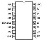
Pinout

  Connection Diagram


Specifications

DC Supply Voltage Range, (VDD) . . . . . . . . . . . . . . . -0.5V to +20V
(Voltage Referenced to VSS Terminals)
Input Voltage Range, All Inputs . . . . . . . . . . . . .-0.5V to VDD +0.5V
DC Input Current, Any One Input . . . . . . . . . . .. . . . . . . . . . .±10mA
Operating Temperature Range. . . . . . . . . . . . . . . . -55 to +125
Package Types D, F, K, H
Storage Temperature Range (TSTG). . . . . . . . . . . -65 to +150
Lead Temperature (During Soldering) . . . . . . . . . . . . . . . . . +265


Description

CD4043BMS types are quad cross-coupled 3-state CMOS NOR latches and the CD4044BMS types are quad cross-coupled 3- state CMOS NAND latches. Each latch has a separate Q output and individual SET and RESET inputs. The Q outputs are controlled by a common ENABLE input. A logic 1 or high on the ENABLE input connects the latch states to the Q outputs. A logic 0 or low on the ENABLE input disconnects the latch states from the Q outputs, results in an open circuit feature allows common busing of the outputs. The CD4043BMS and CD4044BMS are supplied in these 16- lead outline packages: Braze Seal DIP *H4T H4T Frit Seal DIP *H1C HIE Ceramic Flatpack *H3X H6W *CD4043B Only CD4044B Only


Customers Who Bought This Item Also Bought

Margin,quality,low-cost products with low minimum orders. Secure your online payments with SeekIC Buyer Protection.
Resistors
Discrete Semiconductor Products
Motors, Solenoids, Driver Boards/Modules
Prototyping Products
DE1
View more