Features: • High Voltage Type (20V Rating)
• Low Power Consumption: Special CMOS Oscillator Configuration
• Monostable (One-Shot) or Astable (Free-Running) Operation
• True and Complemented Buffered Outputs
• Only One External R and C Required
• Buffered Inputs
• 100% Tested for Quiescent Current at 20V
• Standardized, Symmetrical Output Characteristics
• 5V, 10V and 15V Parametric Ratings
• Meets All Requirements of JEDEC Tentative Standard No. 13B, "Standard Specifications for Description of 'B' Series CMOS Devices"
Application• Envelope Detection
• Frequency Multiplication
• Frequency Division
• Frequency Discriminators
• Timing Circuits
• Time Delay Applications
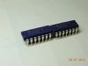
Pinout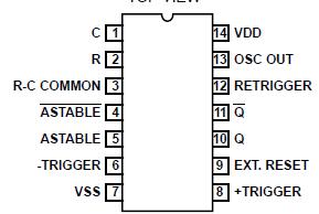
SpecificationsDC Supply Voltage Range, (VDD)..0.5V to +20V (Voltage Referenced to VSS Terminals)
Input Voltage Range, All Inputs .....................................................-0.5V to VDD +0.5V
DC Input Current, Any One Input.......................................................................±10mA
Operating Temperature Range ................. -55 to +125 Package Types D, F, K, H
Storage Temperature Range (TSTG).................................................. -65 to +150
Lead Temperature (During Soldering) ............................................................. +265
At Distance 1/16 ± 1/32 Inch (1.59mm ± 0.79mm) from case for 10s MaximumDescriptionCD4047BMS consists of a gatable astable multivibrator with logic techniques incorporated to permit positive or negative edge triggered monostable multivibrator action with retriggering and external counting options. Inputs include +TRIGGER, -TRIGGER, ASTABLE, ASTABLE, RETRIGGER, and EXTERNAL RESET. Buffered outputs are Q, Q, and OSCILLATOR. In all modes of operation, an external capacitor must be connected between C-Timing and RC-Common terminals, and an external resistor must be connected between the R-Timing and RCCommon terminals. Astable operation is enabled by a high level on the ASTABLE input or a low level on the ASTABLE input, or both. The period of the square wave at the Q and Q Outputs in this mode of operation is a function of the external components employed. CD4047BMS True input pulses on the ASTABLE input or Complement pulses on the ASTABLE input allow the circuit to be used as a gatable multivibrator. The OSCILLATOR output period will be half of the Q terminal output in the astable mode. However, a 50% duty cycle is not guaranteed at this output. The CD4047BMS triggers in the monostable mode when a positive going edge occurs on the +TRIGGER input while the -TRIGGER is held low. Input pulses may be of any duration relative to the output pulse. If retrigger capability is desired, the RETRIGGER input is pulsed. The retriggerable mode of operation is limited to positive going edge. The CD4047BMS will retrigger as long as the RETRIGGER input is high, with or without transitions (See Figure 31) An external countdown option can be implemented by coupling Q to an external N counter and resetting the counter with trigger pulse. The counter output pulse is fed back to the ASTABLE input and has a duration equal to N times the period of the multivibrator. A high level on the EXTERNAL RESET input assures no output pulse during an ON power condition. This input can also be activated to terminate the output pulse at any time. For monostable operation, whenever VDD is applied, an internal power on reset circuit will clock the Q output low within one output period (tM). The CD4047BMS is supplied in these 14-lead outline packages: Braze Seal DIP H4Q Frit Seal DIP H1B Ceramic Flatpack H3W

 CD4047BMS Data Sheet