Features: 15-V Digital or ±7.5-V Peak-to-PeakSwitching
125- Typical On-State Resistance for 15-VOperation
Switch On-State Resistance Matched toWithin 5 Over 15-V Signal-Input Range
On-State Resistance Flat Over FullPeak-to-Peak Signal Range
High On/Off Output-Voltage Ratio: 80 dBTypical at fis = 10 kHz, RL = 1 k
High Degree of Linearity: <0.5% DistortionTypical at fis= 1 kHz, Vis= 5 Vp-p,VDD VSS 10 V, RL = 10 k
Extremely Low Off-State Switch Leakage,Resulting in Very Low Offset Current andHigh Effective Off-State Resistance: 10 pATypical at VDDVSS= 10 V, TA = 25
Extremely High Control Input Impedance(Control Circuit Isolated From SignalCircuit): 1012Typical
Low Crosstalk Between Switches: 50 dBTypical at fis= 8 MHz, RL = 1 k
Matched Control-Input to Signal-OutputCapacitance: Reduces Output SignalTransients
Frequency Response, Switch On = 40 MHzTypical
100% Tested for Quiescent Current at 20 V
5-V, 10-V, and 15-V Parametric Ratings
Meets All Requirements of JEDEC TentativeStandard No. 13-B, Standard Specificationsfor Description of "B" Series CMOSDevices
Application Analog Signal Switching/Multiplexing:
Signal Gating, Modulator, Squelch
Control, Demodulator, Chopper,
Commutating Switch
Digital Signal Switching/Multiplexing
Transmission-Gate Logic Implementation
Analog-to-Digital and Digital-to-AnalogConversion
Digital Control of Frequency, Impedance,Phase, and Analog-Signal Gain
Pinout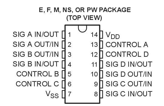 SpecificationsDC supply-voltage range, VDD(voltages referenced to VSSterminal) . . . . . . . .. . . . 0.5 V to 20 V
Input voltage range, Vis(all inputs) . . . . . . . . . . . . . . . . . . . . . . . . . . . . . . . . 0.5 V to VDD+ 0.5 V
DC input current, IIN (any one input) . . . . . . . . . . . . . . . . . . . . . . . . . . . . . . . . . . . . . . . . . ± 10 mA
Package thermal impedance, JA (see Note 1): E package . . . . . . . . . . . . . . . . . . . . . . . . . . 80/W
M package . . . . . . . . . . . . . . . . . . . . . . . . . . 86/W
NS package . . . . . . . . . . . . . . . . . . . . . . . . . 76/W
PW package . . . . . . . . . . .. . . . . . . . . . . . . 113/W
Lead temperature (during soldering):
At distance 1/16 ± 1/32 inch (1,59 ± 0,79 mm) from case for 10 s max . . . . . . . . . . . . . . . . . . 265
Storage temperature range, Tstg . . . . . . . . . . . . . . . . . . . . . . . . . . . . . . . . . . .. . . . . . . .65to 150DescriptionThe CD4066B is a quad bilateral switch intended for the transmission or multiplexing of analog or digital signals.It is pin-for-pin compatible with the CD4016B, but exhibits a much lower on-state resistance. In addition, theon-state resistance is relatively constant over the full signal-input range.
The CD4066B consists of four bilateral switches, each with independent controls. Both the p and the n devicesin a given switch are biased on or off simultaneously by the control signal. As shown in Figure 1, the well of then-channel device on each switch is tied to either the input (when the switch is on) or to VSS(when the switchis off). This configuration eliminates the variation of the switch-transistor threshold voltage with input signal and,thus, keeps the on-state resistance low over the full operating-signal range.
The advantages of CD4066B over single-channel switches include peak input-signal voltage swings equal to the full supplyvoltage and more constant on-state impedance over the input-signal range. However, for sample-and-holdapplications, the CD4016B is recommended.

 CD4066B Data Sheet