CD4097B

DescriptionThe CD4097B is designed as CMOS multiplexer/ demultiplexer which is digitally controlled analog switches having low ON impedance, low OFF leakage current and internal address decoding. In addition, the ON resistance is relatively constant over the full input-signal range.CD4097B has ten...

product image

CD4097B Picture
SeekIC No. : 004311360 Detail

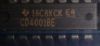
CD4097B: DescriptionThe CD4097B is designed as CMOS multiplexer/ demultiplexer which is digitally controlled analog switches having low ON impedance, low OFF leakage current and internal address decoding. In...

floor Price/Ceiling Price

Part Number:
CD4097B
Supply Ability:
5000

Price Break

  • Qty
  • 1~5000
  • Unit Price
  • Negotiable
  • Processing time
  • 15 Days
Total Cost: $ 0.00

SeekIC Buyer Protection PLUS - newly updated for 2013!

  • Escrow Protection.
  • Guaranteed refunds.
  • Secure payments.
  • Learn more >>

Month Sales

268 Transactions

Rating

evaluate  (4.8 stars)

Upload time: 2024/5/2

Payment Methods

All payment methods are secure and covered by SeekIC Buyer Protection PLUS.

Notice: When you place an order, your payment is made to SeekIC and not to your seller. SeekIC only pays the seller after confirming you have received your order. We will also never share your payment details with your seller.
Product Details

Description


Description

The CD4097B is designed as CMOS multiplexer/ demultiplexer which is digitally controlled analog switches having low ON impedance, low OFF leakage current and internal address decoding. In addition, the ON resistance is relatively constant over the full input-signal range.

CD4097B has ten features. (1)Low ON resistance 125ohms over 15Vp-p signal input range for Vdd-Vss=15V. (2)High OFF resistance channel leakage of +/-10pA. (3)CD4097B Matched switch characteristics which would be typ 5ohms. (4)Very low quiescent power dissipation under all digital control input and supply conditions 0.2uW typ at 10V. (5)CD4097B Binary address decoding on chip. (6)5V, 10V and 15V parametric ratings 100% tested for quiescent current at 20V. (7)Standardized symmetrical output characteristics. (8)Maximum input current of 1uA at 18V over all package. (9)100% tested for quiescent current at 20V. (10)Meets all requirements of JEDEC tentative standard No.13B. Those are all the main features.

Some absolute maximum ratings have been concluded into several points as follow. (1)CD4097B's DC supply voltage range would be from -0.5V to 20V. (2)Its input voltage range all inputs would be from -0.5V to Vdd+0.5V. (3)Its DC input current any one input would be +/-10mA. (4)Its power dissipation per package would be 500mW. (5)Its device dissipation per output transistor would be 100mW. (6)Its operating temperature range would be from -55°C to 125°C. (7)Its storage temperature range would be from -65°C to 150°C. (8)Its lead temperature would be 265°C. CD4097B should be noted that stresses above those listed in absolute maximum ratings may cause permanent damage to CD4097B.

Also some electrical characteristics of CD4097B are concluded as follow. (1)Its quiescent device current would be typ 0.04uA and max 5uA at Vdd=5V. (2)Its ON-state resistance would be typ 470ohms and max 1050ohms at Vdd=5V. (3)CD4097B's change in on-state resistance would be typ 15ohms at Vdd=5V. (4)Its input low voltage max would be 1.5V at Vdd=5V. (5)Its input high voltage min would be 3.5V at Vdd=5V. And so on. If you have any question or suggestion or want to know more CD4097B information please contact us for details. Thank you!


Customers Who Bought This Item Also Bought

Margin,quality,low-cost products with low minimum orders. Secure your online payments with SeekIC Buyer Protection.
Potentiometers, Variable Resistors
Optoelectronics
LED Products
Line Protection, Backups
Resistors
Discrete Semiconductor Products
View more