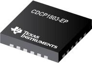
DescriptionThe CDCP1803 clock driver distributes one pair of differential clock inputs to three pairs of LVPECL differential clock outputs Y[2:0] and Y[2:0], with minimum skew for clock distribution. The CDCP1803 is specifically designed for driving 50- transmission lines.The CDCP1803 has three control pins, S0, S1, and S2, to select different output mode settings, see Table 1 for details. The CDCP1803 is characterized for operation from -40°C to 85°C.For use in single-ended driver applications, the CDCP1803 also provides a VBB output pin that can be directly connected to the unused input as a common-mode voltage reference.
Features of the CDCP1803 are:(1)distributes one differential clock input to three LVPECL differential clock outputs; (2)programmable output divider for two LVPECL outputs; (3)low-output skew 15 ps (Typical); (4)Vcc Range 3 V-3.6 V; (5)signaling rate up to 800-MHz LVPECL; (6)differential input stage for wide common-mode range; (7)provides vbb bias voltage output for single-ended input signals; (8)receiver input threshold 75 mV; (9)24-Pin MLF package (4 mm x 4 mm); (10)accepts any differential signaling: LVDS,HSTL, CML, VML, SSTL-2, and single-ended: LVTTL/LVCMOS.
The absolute maximum ratings of the CDCP1803 can be summarized as:(1)supply voltage:-0.3 to 3.8V;(2)storage temperature:-65 to 150;(3)maximum junction temperature:125;(4)input voltage:-0.2 to Vdd+0.2;(5)moisture level 24-pin MLF package:2.Stresses beyond those listed under "absolute maximum ratings" may cause permanent damage to the device. These are stress ratings only, and functional operation of the device at these or any other conditions beyond those indicated under "recommended operating conditions" is not implied. Exposure to absolute-maximum-rated conditions for extended periods may affect device reliability.TI warrants performance of its hardware products to the specifications applicable at the time of sale in accordance with TI's standard warranty. Testing and other quality control techniques are used to the extent TI deems necessary to support this warranty. Except where mandated by government requirements, testing of all parameters of each product is not necessarily performed.

 CDCP1803 Data Sheet


