CDP1852

Features: • Static Silicon-Gate CMOS Circuitry• Parallel 8-Bit Data Register and Buffer• Handshaking Via Service Request Flip-Flop• Low Quiescent and Operating Power• Interfaces Directly with CDP1800-Series Microprocessors• Single Voltage Supply• Full Mili...

product image

CDP1852 Picture
SeekIC No. : 004312443 Detail

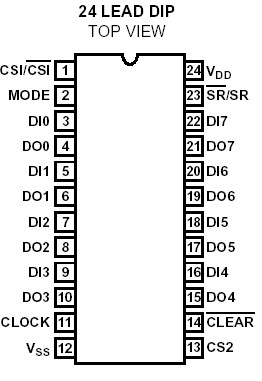
CDP1852: Features: • Static Silicon-Gate CMOS Circuitry• Parallel 8-Bit Data Register and Buffer• Handshaking Via Service Request Flip-Flop• Low Quiescent and Operating Power• I...

floor Price/Ceiling Price

Part Number:
CDP1852
Supply Ability:
5000

Price Break

  • Qty
  • 1~5000
  • Unit Price
  • Negotiable
  • Processing time
  • 15 Days
Total Cost: $ 0.00

SeekIC Buyer Protection PLUS - newly updated for 2013!

  • Escrow Protection.
  • Guaranteed refunds.
  • Secure payments.
  • Learn more >>

Month Sales

268 Transactions

Rating

evaluate  (4.8 stars)

Upload time: 2024/5/9

Payment Methods

All payment methods are secure and covered by SeekIC Buyer Protection PLUS.

Notice: When you place an order, your payment is made to SeekIC and not to your seller. SeekIC only pays the seller after confirming you have received your order. We will also never share your payment details with your seller.
Product Details

Description


Features:

• Static Silicon-Gate CMOS Circuitry
• Parallel 8-Bit Data Register and Buffer
• Handshaking Via Service Request Flip-Flop
• Low Quiescent and Operating Power
• Interfaces Directly with CDP1800-Series Microprocessors
• Single Voltage Supply
• Full Military Temperature Range (-55oC to +125oC)


Pinout

  Connection Diagram


Specifications

DC Supply-voltage Range, (VDD) (Voltage Referenced to VSS Terminal) CDP1852 . . . . . . . . . . . . .  . . . . . . . . . . . -0.5 to +11V
CDP1852C . . . . . . . . . . . . . . . . . . . . . . . . . . . . . . . . . . . . . . . . .. . . . . . .. . . . . . .. . . . . . .. . . . . . .. . . . . . .. . . . . -0.5 to +7V
Input Voltage Range, All Inputs . . . . . . . . . . . . . .  . . . . . . . . . . . . . . . . . . . . . . . . . . . . . . . . . . . . . . . . . . . . -0.5 to VDD +0.5V
DC Input Current, Any One Input . . . . . . . . . . . . . . . . . . . . . . . .  . . . . . . . . . . . . . . . . . . . . . . . . . . . . . . . . . . . . . . . . . ±10mA
Device Dissipation Per Output Transistor. . . . . . . . . . . . . . .  . . . . .. . . . .. . . . .. . . . .. . . . .. . . . .. . . . . . . . .. . . . .. . . . .100mW
For TA = Full Package-Temperature Range (All Package Type)


Description

The CDP1852 and CDP1852C are parallel, 8-bit, mode-programmable input/output ports. They are compatible and will interface directly with CDP1800-series microprocessors. They are also useful as 8-bit address latches when used with the CDP1800 multiplexed address bus and as I/O ports in generalpurpose applications.
The mode control is used to program CDP1852 as an input port (mode = 0) or as an output port (mode = 1). The SR/SR output can be used as a signal to indicate when data is ready to be transferred. In the input mode, a peripheral device can strobe data into the CDP1852, and microprocessor can read that data by device selection. In the output mode, a microprocessor strobes data into the CDP1852, and handshaking is established with a peripheral device when the CDP1852 is deselected. In the input mode, data at the data-in terminals (DI0-DI7) is strobed into the port's 8-bit register by a high (1) level on the clock line. The negative high-to-low transition of the clock latches the data in the register and sets the service request output low (SR/SR = 0). When CS1/CS1 and CS2 are high (CS1/CS1 and CS2 = 1), the three-state output drivers are enabled and data in the 8-bit register appear at the data-out terminals (D00-D07). When either CS1/CS1 or CS2 goes low (CS1/CS1 or CS2 = 0), the data-out terminals are three-stated and the service request output returns high (SR/SR =1). In the output mode, the output drivers are enabled at all times. Data at the data-in terminals (DI0-DI7) is strobed into the 8-bit register when CS1/CS1 is low (CS1/CS1 = 0) and CS2 and the clock are high (1), and are present at the data-out terminals (D00-D07). The negative high-to-low transition of the clock latches the data in the register. The SR/SR output goes high (SR/SR = 1) when the device is deselected (CS1/CS1 = 1 or CS2 = 0) and returns low (SR/SR = 0) on the following trailing edge of the clock.


Customers Who Bought This Item Also Bought

Margin,quality,low-cost products with low minimum orders. Secure your online payments with SeekIC Buyer Protection.
Hardware, Fasteners, Accessories
Memory Cards, Modules
Cables, Wires - Management
Transformers
Power Supplies - External/Internal (Off-Board)
View more