Features: • Factory-EPROM configurable for quick availability and prototyping.
• General purpose clock synthesizer for all applications
such as modems, disk drives, CD-ROM drives, Video CD players, games, set-top boxes, data/telecommunications, etc.
• Three independent configurable clock outputs
• Outputs ranging from 500 kHz to 100 MHz (5V) and up to 80 MHz for 3.3V operation
• Configurable output control pin (pin 8) can be used as an output enable, power-down, suspend or select line.
• Phase-locked loop oscillator input derived from external crystal (10 MHz to 25 MHz) or external reference clock (1 MHz to 30 MHz)
• 3.3V or 5V operation (factory configured)
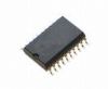
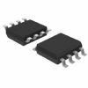
• 8-pin 150-mil packaging achieves minimum footprint for space-critical applications
• Sophisticated internal loop filter requires no external components or manufacturing tweaks as commonly required with external filtersPinout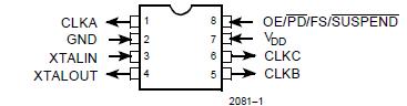 Specifications(Above which the useful life may be impaired. For user guidelines,
not tested.)
Supply Voltage............................................. 0.5V to +7.0V
DC Input Voltage ....................................0.5V to VDD+0.5V
Storage Temperature ................................ 65 to +150
Max. Soldering Temperature (10 sec) ..........................260
Junction Temperature ..................................................150
Static Discharge Voltage ..........................................>2000V
(per MIL-STD-883, Method 3015)DescriptionThe CY2081 is a general-purpose clock synthesizer designed for use in applications such as modems, disk drives, CD-ROM drives, Video CD players, games, set-top boxes and data/telecommunications.
This devices offers three configurable clock outputs in an 8-pin 150-mil SOIC package and can be configured to operate off either a 3.3V or 5V power supply. The on-chip reference oscillator is designed for 10 MHz to 25 MHz crystals. Alternatively, a reference clock between 1 MHz and 30 MHz can be used.
The CY2081 also features an output control pin (pin 8) which can be configured as an output enable, power down, frequency select, or suspend input. This gives the user the ability to three-state the output, power down the device, change the CLKA output frequency during operation, or suspend any of the outputs. Asserting thePD input will result in all the PLLs and the outputs being shut down. The PLLs will have to re-lock when the PD input is deasserted.
The CY2081 outputs three clocks: CLKA, CLKB, and CLKC, whose frequencies can possess any value within the specified range. Additionally, the reference frequency can be obtained on any output. Custom configurations with user-defined features and frequencies can be obtained by filling out the custom configuration form located at the back of this data sheet and contacting your local Cypress representative.
The CY2081 can replace multiple Metal Can Oscillators (MCO) in a synchronous system, providing cost and board space savings to manufacturers. Hence, this device is ideally suited for applications that require multiple, accurate, and stable clocks synthesized from low-cost generators in small packages.
A hard disk drive is an example of such an application.
In this case, CLKA drives the PLL in the Read Controller, while CLKB and CLKC drive the MCU and associated sequencers.
Consider using the CY2291, CY2292, or CY2907 for applications that require more than three output clocks.

 CY2081 Data Sheet