CY2SSTV16859

Features: • Differential clock inputs up to 280 MHz• Supports LVTTL switching levels on the RESET# pin• Output drivers have controlled edge rates, so no external resistors are required.• Two KV ESD protection• Latch-up performance exceeds 100 mA per JESD78, Class II&#...

product image

CY2SSTV16859 Picture
SeekIC No. : 004319305 Detail

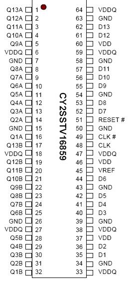
CY2SSTV16859: Features: • Differential clock inputs up to 280 MHz• Supports LVTTL switching levels on the RESET# pin• Output drivers have controlled edge rates, so no external resistors are requ...

floor Price/Ceiling Price

Part Number:
CY2SSTV16859
Supply Ability:
5000

Price Break

  • Qty
  • 1~5000
  • Unit Price
  • Negotiable
  • Processing time
  • 15 Days
Total Cost: $ 0.00

SeekIC Buyer Protection PLUS - newly updated for 2013!

  • Escrow Protection.
  • Guaranteed refunds.
  • Secure payments.
  • Learn more >>

Month Sales

268 Transactions

Rating

evaluate  (4.8 stars)

Upload time: 2024/4/26

Payment Methods

All payment methods are secure and covered by SeekIC Buyer Protection PLUS.

Notice: When you place an order, your payment is made to SeekIC and not to your seller. SeekIC only pays the seller after confirming you have received your order. We will also never share your payment details with your seller.
Product Details

Description


Features:

• Differential clock inputs up to 280 MHz
• Supports LVTTL switching levels on the RESET# pin
• Output drivers have controlled edge rates, so no
   external resistors are required.
• Two KV ESD protection
• Latch-up performance exceeds 100 mA per JESD78, Class II
• 64-pin TSSOP/JEDEC and 56-pin QFN package availability
• JEDEC specification supported


Pinout

  Connection Diagram


Specifications

Parameter Description Condition Min. Max. Unit
VTERM
Terminal Voltage with respect to VSS   -0.5 3.6 V
VTERM Terminal Voltage with respect to VSS   -0.5 VDD + 0.5 V
TSTG Storage Temperature   65° 150°C °C
IOUT DC Output Current   -50 50 mA
IIK Continuous Clamp Current VI<0 or VI>VSS -50 50 mA
IOK Continuous Clamp Current VO<0 or VO>VDD -50 50 mA
Idd
ISS
Continuous Current through each VDD, VDDQ or VSS   -100 100 mA


Description

This 13-bit to 26-bit registered buffer is designed for 2.3V to 2.7 VDD operations.

All inputs are compatible with the JEDEC Standard for SSTL-2, except the LVCMOS reset (RESET#) input. All outputs are SSTL_2, Class II compatible.

The CY2SSTV16859 operates from a differential clock (CLK and CLK#) of frequency up to 280 MHz. Data are registered at crossing of CLK going high and CLK# going low When RESET# is low, the differential input receivers are disabled, and undriven (floating) data and clock inputs are allowed. The LVCMOS RESET# input must always be held at a valid logic high or low level.

To ensure defined outputs from the register before a stable clock has been supplied, RESET# must be held in the low state during power up.

In the DDR DIMM application, RESET# is completely asynchronous with respect to CLK# and CLK. Therefore, no timing relationship can be guaranteed between the two. When entering reset, the register is cleared and the outputs are driven low quickly, relative to the time to disable the differential input receivers, thus ensuring no glitches on the output.

However, when coming out of reset, the register becomes active quickly, relative to the time to enable the differential input receivers.


Customers Who Bought This Item Also Bought

Margin,quality,low-cost products with low minimum orders. Secure your online payments with SeekIC Buyer Protection.
Hardware, Fasteners, Accessories
Power Supplies - Board Mount
Soldering, Desoldering, Rework Products
Cable Assemblies
Batteries, Chargers, Holders
RF and RFID
View more