Features: • Differential Clock Inputs up to 280 MHz
• Supports LVTTL switching levels on theRESET pin
• Output drivers have controlled edge rates, so no external resistors are required
• Two KV ESD protection
• Latch-up performance exceeds 100 mA: JESD78, Class II
• Conforms to JEDEC STD (JESD82-3) for buffered DDR DIMMs
• 48-pin TSSOPPinout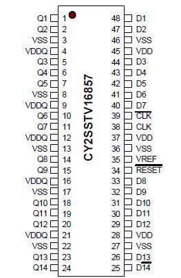 Specifications
|
Parameter |
Description |
Condition |
Min. |
Max. |
Unit |
|
VDD |
Supply Voltage[4] |
Non-functional |
2.3 |
2.7 |
VDC |
|
VDD |
Operating Voltage[4] |
Functional |
2.3 |
2.7 |
VDC |
|
Vin |
Input Voltage |
Relative to VSS |
0 |
VDD |
VDC |
|
Vout |
Output Voltage |
Relative to VSS |
|
VDDQ |
VDC |
|
IOUT |
DC Output Current |
|
|
±50 |
mA |
|
IIK |
Continuous Clamp Current |
VI < 0 or VI > VSS |
|
±50 |
mA |
|
IOK |
Continuous Clamp Current |
VO < 0 |
|
50 |
mA |
|
IDD/ISS |
Continuous current through each VDD or VSS |
|
|
±100 |
mA |
|
LUI |
Latch Up Immunity |
Exceeds spec of |
100 |
mA |
|
RPS |
Power Supply Ripple |
Ripple Frequency < 100 kHz |
|
150 |
mVp-p |
|
Ts |
Temperature, Storage |
Non-functional |
65 |
+150 |
°C |
|
Ta |
Temperature, Operating Ambient |
Functional |
0 |
+70 |
°C |
|
Tj |
Temperature, Junction |
Functional |
|
165 |
°C |
|
ØJc |
Dissipation, Junction to Case |
Mil-Spec 883E Method 1012.1 |
22.23 |
°C/W |
|
ØJA |
Dissipation, Junction to Ambient |
JEDEC (JESD 51) |
74.52 |
°C/W |
|
ULFL |
Flammability |
By design and verification |
V 0 |
Grade |
|
MSL |
Moisture Sensitivity |
By design and verification |
MSL 1 |
Grade |
|
ESDh |
ESD Protection (Human Body Model) |
|
2000 |
|
V |
DescriptionThis 14-bit registered buffer is designed specifically for 2.3V to 2.7V VDD operation and is characterized for operation from 0°C to + 85°C.
All inputs are compatible with the JEDEC Standard for SSTL_2, except the LVCMOS reset (RESET) input. All outputs are SSTL_2, Class II-compatible.
The SSTV16857 operates from a differential clock (CLK and CLK). Data is measured at the crossing of CLK going HIGH, and CLK going LOW.
When RESET is LOW, the differential input receivers are disabled, and undriven (floating) data, clock, and REF voltage inputs are allowed. In addition, when RESET is LOW, all registers are reset and all outputs force to the LOW state. The LVCMOSRESET input must always be held at a valid logic HIGH or LOW level.
To ensure defined outputs from the register before a stable clock has been supplied, RESET must be held in the LOW state during power-up.
In the DDR registered DIMM application, RESET is specified to be completely asynchronous with respect to CLK and CLK. Therefore, no timing relationship can be guaranteed between the two. When entering reset, the register will be cleared and the outputs will be driven LOW quickly, relative to the time to disable the differential input receivers, thus ensuring no glitches on the output. However, when coming out of reset, the register will become active quickly, relative to the time to enable the differential input receivers. As long as the data inputs are low, and the clock is stable during the time from the LOW-to-HIGH transition of RESET until the input receivers are fully enabled, the design must ensure that the outputs will remain LOW.

 CY2SSTV16857 Data Sheet