Features: • True dual-ported memory cells that allow simultaneous access of the same memory location
• Synchronous pipelined operation
• Organization of 1-Mbit, 2-Mbit, 4-Mbit and 9-Mbit devices
• Pipelined output mode allows fast operation
• 0.18-micron CMOS for optimum speed and power
• High-speed clock to data access
• 3.3V low power
-Active as low as 225 mA (typ)
-Standby as low as 55 mA (typ)
• Mailbox function for message passing
• Global master reset
• Separate byte enables on both ports
• Commercial and industrial temperature ranges
• IEEE 1149.1-compatible JTAG boundary scan
• 172-ball FBGA (1 mm pitch) (15 mm * 15 mm)
• 176-pin TQFP (24 mm * 24 mm * 1.4 mm)
• Counter wrap around control
-Internal mask register controls counter wrap-around
-Counter-interrupt flags to indicate wrap-around
-Memory block retransmit operation
• Counter readback on address lines
• Mask register readback on address lines
• Dual Chip Enables on both ports for easy depth expansion
Pinout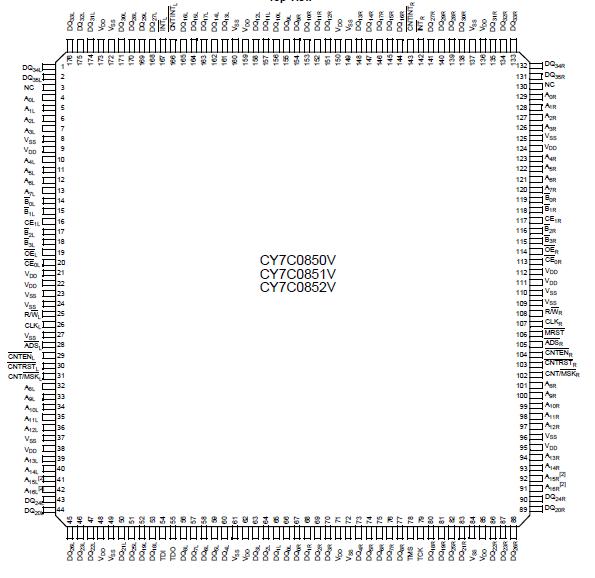 SpecificationsStorage Temperature ......................................................................... 65°C to + 150°C
Ambient Temperature with Power Applied............................................55°C to + 125°C
Supply Voltage to Ground Potential ........................................................ 0.5V to + 4.6V
DC Voltage Applied to Outputs in High-Z State.................................0.5V to VDD + 0.5V
DC Input Voltage ...................................................................... 0.5V to VDD + 0.5V[16]
Output Current into Outputs (LOW)....................................................................... 20 mA
Static Discharge Voltage......................................................................................> 2000V
(JEDEC JESD22-A114-2000B) Latch-up Current................................................. > 200 mADescriptionThe FLEx36 family includes 1M, 2M, 4M and 9M pipelined, synchronous, true dual-port static RAMs that are high-speed, low-power 3.3V CMOS. Two ports are provided, permitting independent, simultaneous access to any location in memory. The result of writing to the same location by more than one port at the same time is undefined. Registers on control, address, and data lines of CY7C0852V allow for minimal set-up and hold time.
During a Read operation, data of CY7C0852V is registered for decreased cycle time. Each port contains a burst counter on the input address register. After externally loading the counter with the initial address, the counter will increment the address internally (more details to follow). The internal Write pulse width is independent of the duration of the R/W input signal. The internal Write pulse is self-timed to allow the shortest possible cycle times.
A HIGH onCE0 or LOW on CE1 for one clock cycle will power down the internal circuitry to reduce the static power consumption. One cycle with chip enables asserted is required to reactivate the outputs.
Additional features of CY7C0852V include: readback of burst-counter internal address value on address lines, counter-mask registers to control the counter wrap-around, counter interrupt (CNTINT) flags, readback of mask register value on address lines, retransmit functionality, interrupt flags for message passing, JTAG for boundary scan, and asynchronous Master Reset (MRST).
The CY7C0853 device in this family has limited features. Please see See "Address Counter and Mask Register Operations[10]" on page 8. for details.

 CY7C0852V Data Sheet


