Features: Fully registered inputs and outputs for pipelined oper-
ation
128K by 36 common I/O architecture
3.3V core power supply
2.5V/3.3V I/O operation
Fast clock-to-output times
- 2.6 ns (for 250-MHz device)
- 2.6 ns (for 225-MHz device)
- 2.8 ns (for 200-MHz device)
- 3.5 ns (for 166-MHz device)
- 4.0 ns (for 133-MHz device)
(C)
User-selectable burst counter supporting Intel
(C)
Pentium interleaved or linear burst sequences
Separate processor and controller address strobes
Synchronous self-timed writes
Asynchronous output enable
JEDEC-standard 100-pin TQFP, 119-pin BGA and
165-pin fBGA packages
"ZZ" Sleep Mode option and Stop Clock option
Available in Industrial and Commercial temperature
rangesPinout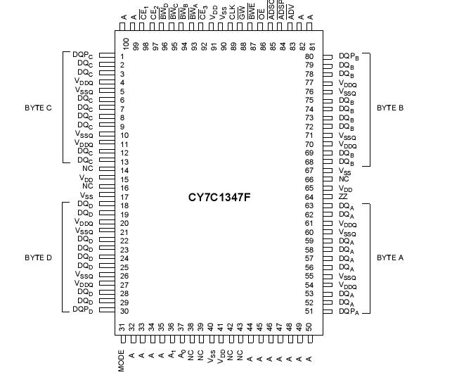 Specifications
Storage Temperature ......................................-65°C to +150°C
Ambient Temperature with
Power Applied..................................................-55°C to +125°C
Supply Voltage on V Relative to GND.....................-0.5V to +4.6V
DC Voltage Applied to Outputs
in High-Z State...............................................-0.5V to V DD + 0.5V
DC Input Voltage...........................................-0.5V to V DD + 0.5V
Current into Outputs (LOW)................................................20 mA
Static Discharge Voltage................................................. > 2001V
(per MIL-STD-883, Method 3015)
Latch-up Current........................................................... > 200 mA
DescriptionThe CY7C1347F is a 3.3V, 128K by 36 synchronous-pipelined SRAM designed to support zero-wait-state secondary cache with minimal glue logic.
CY7C1347F I/O pins can operate at either the 2.5V or the 3.3V level, the I/O pins are 3.3V tolerant when VDDQ = 2.5V.
All synchronous inputs of CY7C1347F pass through input registers controlled by the rising edge of the clock. All data outputs pass through output registers controlled by the rising edge of the clock. Maximum access delay from the clock rise is 2.6 ns (250-MHz device)
CY7C1347F supports either the interleaved burst sequence used by the Intel Pentium processor or a linear burst sequence (R) used by processors such as the PowerPC . The burstsequence is selected through the MODE pin. Accesses can be initiated by asserting either the Address Strobe from Processor (ADSP) CY7C1347F or the Address Strobe from Controller (ADSC) at clock rise. Address advancement through the burst sequence is controlled by the ADV input. A 2-bit on-chip wraparound burst counter captures the first address in a burst sequence and automatically increments the address for the rest of the burst access.
Byte write operations of CY7C1347F are qualified with the four Byte Write Select (BW [A:D]) inputs. A Global Write Enable (GW) overrides all byte write inputs and writes data to all four bytes. All writes are conducted with on-chip synchronous self-timed writecircuitry.
Three synchronous Chip Selects CY7C1347F(CE1 , CE2 , CE 3) and an asynchronous Output Enable (OE ) provide for easy bank selection and output three-state control. In order to provide proper data during depth expansion, OE is masked during the first clock of a read cycle when emerging from a deselected state.

 CY7C1347F Data Sheet


