Features: •Pin compatible and functionally equivalent to ZBT™ devices
•Internally self-timed output buffer control to eliminate the need to use OE
•Byte Write capability
•256K x 18 common I/O architecture
•Single 3.3V power supply
•2.5V / 3.3V I/O Operation
•Fast clock-to-output times
•2.6 ns (for 250-MHz device)
•2.8 ns (for 200-MHz device)
•3.5 ns (for 166-MHz device)
•4.0 ns (for 133-MHz device)
•Clock Enable (CEN) pin to suspend operation
•Synchronous self-timed writes
•Asynchronous output enable (OE)
•Pb-Free 100 TQFP package
•Burst Capability-linear or interleaved burst order
•ZZ" Sleep Mode Option and Stop Clock option
Pinout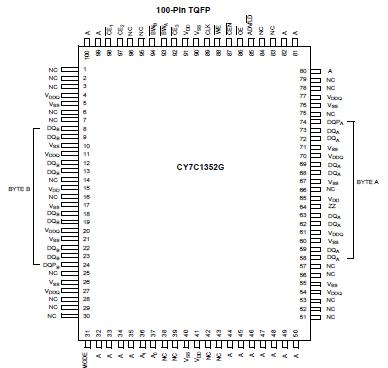 Specifications
(Above which the useful life may be impaired. For user guidelines,
not tested.)
Storage Temperature ..................................... ....................−65°C to +150°C
Ambient Temperature with
Power Applied..................................................................... −55°C to +125°C
Supply Voltage on VDD Relative to GND......................................−0.5V to +4.6V
DC Voltage Applied to Outputs
in tri-state........................................................................−0.5V to VDDQ + 0.5V
DC Input Voltage .............................................................. −0.5V to VDD + 0.5V
Current into Outputs (LOW)..................................................................... 20 mA
Static Discharge Voltage.......................................... .............................> 2001V
(per MIL-STD-883, Method 3015)
Latch-up Current................................................................................. > 200 mA
DescriptionThe CY7C1352G is a 3.3V, 256K x 18 synchronous-pipelined Burst SRAM designed specifically to support unlimited true back-to-back Read/Write operations without the insertion of wait states. The CY7C1352G is equipped with the advanced No Bus Latency™ (NoBL™) logic required to enable consecutive Read/Write operations with data being transferred on every clock cycle. This feature dramatically improves the throughput of the SRAM, especially in systems that require frequent Write/Read transitions.
All synchronous inputs of CY7C1352G pass through input registers controlled by the rising edge of the clock. All data outputs of CY7C1352G pass through output registers controlled by the rising edge of the clock. The clock input is qualified by the Clock Enable (CEN) signal, which, when deasserted, suspends operation and extends the previous clock cycle. Maximum access delay from the clock rise is 2.6 ns (250-MHz device).
Write operations of CY7C1352G are controlled by the two Byte Write Select (BW[A:B]) and a Write Enable (WE) input. All writes are conducted with on-chip synchronous self-timed write circuitry.
Three synchronous Chip Enables (CE1, CE2, CE3) and an asynchronous Output Enable (OE )of CY7C1352G provide for easy bank selection and output tri-state control. In order to avoid bus contention, the output drivers are synchronously tri-stated during the data portion of a write sequence

 CY7C1352G Data Sheet


