Features: • Supports 133-MHz bus operations
• 512K X 36/1M X 18 common I/O
• 3.3V 5% and +10% core power supply (VDD)
• 2.5V or 3.3V I/O supply (VDDQ)
• Fast clock-to-output times
-6.5 ns (133-MHz version)
-7.5 ns (117-MHz version)
-8.5 ns (100-MHz version)
• Provide high-performance 2-1-1-1 access rate
• User-selectable burst counter supporting Intel® Pentium interleaved or linear burst sequences
• Separate processor and controller address strobes
• Synchronous self-timed write
• Asynchronous output enable
• Offered in JEDEC-standard 100-pin TQFP ,119-ball BGA and 165-ball fBGA packages
• JTAG boundary scan for BGA and fBGA packages
• "ZZ" Sleep Mode optionPinout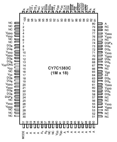
SpecificationsStorage Temperature .................................65°C to +150°C
Ambient Temperature with
Power Applied.............................................55°C to +125°C
Supply Voltage on VDD Relative to GND........... 0.3V to +4.6V
DC Voltage Applied to Outputs
in Tri-State..............................................0.5V to VDDQ + 0.5V
DC Input Voltage.......................................0.5V to VDD + 0.5V
Current into Outputs (LOW)............................................ 20 mA
Static Discharge Voltage............................................... >2001V
(per MIL-STD-883, Method 3015)
Latch-up Current........................................................ >200 mADescription
The CY7C1381C/CY7C1383C is a 3.3V, 512K x 36 and 1M x 18 Synchronous Flowthrough SRAMs, respectively designed to interface with high-speed microprocessors with minimum glue logic. Maximum access delay from clock rise is 6.5 ns (133-MHz version). A 2-bit on-chip counter captures the first address in a burst and increments the address automatically for the rest of the burst access. All synchronous inputs are gated by registers controlled by a positive-edge-triggered Clock Input (CLK). The synchronous inputs include all addresses, all data inputs, address-pipelining Chip Enable (CE1), depth-expansion Chip Enables (CE2 and CE3 [2]), Burst
Control inputs (ADSC, ADSP, and ADV), Write Enables (BWx, and BWE), and Global Write (GW). Asynchronous inputs include the Output Enable (OE) and the ZZ pin.
The CY7C1381C/CY7C1383C allows either interleaved or linear burst sequences, selected by the MODE input pin. A HIGH selects an interleaved burst sequence, while a LOW selects a linear burst sequence. Burst accesses can be initiated with the Processor Address Strobe (ADSP) or the cache Controller Address Strobe (ADSC) inputs. Address advancement is controlled by the Address Advancement (ADV) input.
Addresses and chip-enables of CY7C1381C/CY7C1383C are registered at rising edge of clock when either Address Strobe Processor (ADSP) or Address Strobe Controller (ADSC) are active. Subsequent burst addresses can be internally generated as controlled by the Advance pin (ADV).
The CY7C1381C/CY7C1383C operates from a +3.3V core power supply while all outputs may operate with either a +2.5 or +3.3V supply. All inputs and outputs are JEDEC-standard JESD8-5-compatible.

 CY7C1383C Data Sheet


