Features: •3.3V operation for low power consumption and easy integration into low-voltage systems
•High-speed, low-power, first-in first-out (FIFO) memories
•16K * 9 (CY7C4261V)
•32K * 9 (CY7C4271V)•64K * 9 (CY7C4281V)
•128K * 9 (CY7C4291V)
•0.35-micron CMOS for optimum speed/power
•High-speed 100-MHz operation (10-ns read/write cycle times)
•Low power
-I CC = 25 mA
-I SB = 4 mA
•Fully asynchronous and simultaneous read and write operation
•Empty, Full, and programmable Almost Empty and Almost Full status flags
•Output Enable (OE ) pin
•Independent read and write enable pins
•Supports free-running 50% duty cycle clock inputs
•Width- Expansion capability
•32-pin PLCC
•Pin-compatible density upgrade to CY7C42X1V family
•Pin-compatible 3.3V solutions for CY7C4261/71/81/91Pinout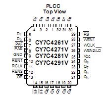 Specifications(Above which the useful life may be impaired. For user guide-
lines, not tested.)
Storage Temperature ...................................65°C to +150°C
Ambient Temperature with
Power Applied...............................................55°C to +125°C
Supply Voltage to Ground Potential.....................0.5V to +3.6V
DC Voltage Applied to Outputs
in High-Z State..........................................0.5V to V CC + 0.5V
DC Input Voltage......................................0.5V to V CC + 0.5V
Output Current into Outputs (LOW)...................................20 mA
Static Discharge Voltage.................................................> 2001V
(per MIL-STD-883, Method 3015)
Latch-up Current...........................................................> 200 mADescriptionThe CY7C4261/71/81/91V are high-speed, low-power FIFO memories with clocked read and write interfaces. All are nine bits wide. TheCY7C4261/71/81/91V are pin-compatible to the CY7C42x1V Synchronous FIFO family. Programmable features include Almost Full/Almost Empty flags. The CY7C4261/71/81/91V provide solutions for a wide variety of data bffering needs, including high-speed data acquisition, multiprocessor inter-faces, and communications buffering.
The CY7C4261/71/81/91V have 9-bit input and output ports that are controlled by separate clock and enable signals. The input port is controlled by a free-running clock (WCLK) and two write-enable pins (WEN1 , WEN2/LD ).
When WEN1 is LOW and WEN2/LD is HIGH, data is written into the FIFOof the CY7C4261/71/81/91V on the rising edge of the WCLK signal. While WEN1 and WEN2/LD are held active, data is continually written into the FIFO on each WCLK cycle. The output port is controlled in a similar manner by a free-running read clock (RCLK) and two read enable pins (REN1 , REN2 ). In addition, the CY7C4261/71/81/91V has an output enable pin (OE ). The read (RCLK) and write (WCLK) clocks may be tied together for single-clock operation or the two clocks may be run indepen- dently for asynchronous read/write applications. Clock frequencies up to 100 MHz are achievable. Depth expansion is possible using one enable input for system control, while the other enable is controlled by expansion logic to direct the flow of data.

 CY7C4281V Data Sheet


