DS92LV090A

Features: ·Bus LVDS Signaling·3.2 nanosecond propagation delay max·Chip to Chip skew ±800ps·Low power CMOS design·High Signaling Rate Capability (above 100 Mbps)·0.1V to 2.3V Common Mode Range for VID = 200mV·±100 mV Receiver Sensitivity·Supports open and terminated failsafe on port pins·3.3V oper...

product image

DS92LV090A Picture
SeekIC No. : 004329429 Detail

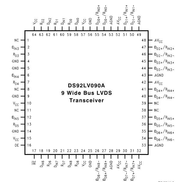
DS92LV090A: Features: ·Bus LVDS Signaling·3.2 nanosecond propagation delay max·Chip to Chip skew ±800ps·Low power CMOS design·High Signaling Rate Capability (above 100 Mbps)·0.1V to 2.3V Common Mode Range for V...
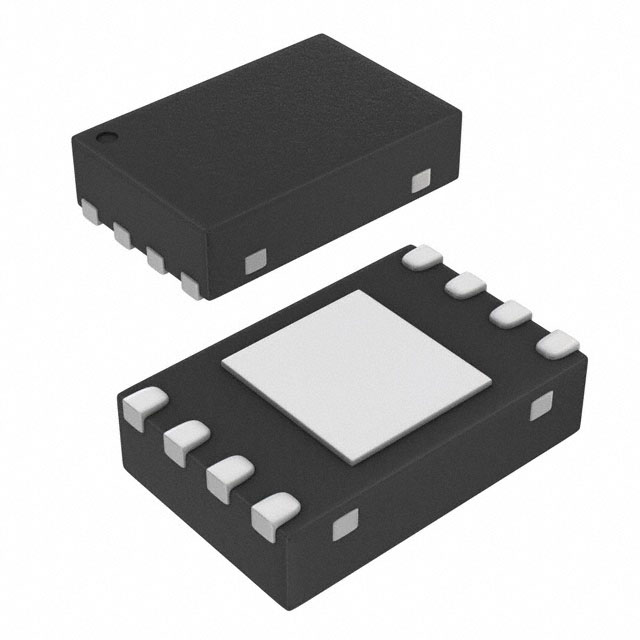
floor Price/Ceiling Price

Part Number:
DS92LV090A
Supply Ability:
5000

Price Break

  • Qty
  • 1~5000
  • Unit Price
  • Negotiable
  • Processing time
  • 15 Days
Total Cost: $ 0.00

SeekIC Buyer Protection PLUS - newly updated for 2013!

  • Escrow Protection.
  • Guaranteed refunds.
  • Secure payments.
  • Learn more >>

Month Sales

268 Transactions

Rating

evaluate  (4.8 stars)

Upload time: 2024/4/26

Payment Methods

All payment methods are secure and covered by SeekIC Buyer Protection PLUS.

Notice: When you place an order, your payment is made to SeekIC and not to your seller. SeekIC only pays the seller after confirming you have received your order. We will also never share your payment details with your seller.
Product Details

Description


Features:

·Bus LVDS Signaling
·3.2 nanosecond propagation delay max
·Chip to Chip skew ±800ps
·Low power CMOS design
·High Signaling Rate Capability (above 100 Mbps)
·0.1V to 2.3V Common Mode Range for VID = 200mV
·±100 mV Receiver Sensitivity
·Supports open and terminated failsafe on port pins
·3.3V operation
·Glitch free power up/down (Driver & Receiver disabled)
·Light Bus Loading (5 pF typical) per Bus LVDS load
·Designed for Double Termination Applications
·Balanced Output Impedance
·Product offered in 64 pin TQFP package
·High impedance Bus pins on power off (VCC = 0V)
·Driver Channel to Channel skew (same device) 230ps typical
·Receiver Channel to Channel skew (same device) 370ps typical


Pinout

  Connection Diagram


Specifications

Supply Voltage (VCC)                                                                     4.0V
Enable Input Voltage (DE, RE)                             −0.3V to (VCC +0.3V)
Driver Input Voltage (DIN)                                   −0.3V to (VCC +0.3V)
Receiver Output Voltage (ROUT)                          −0.3V to (VCC +0.3V)
Bus Pin Voltage (DO/RI±)                                              −0.3V to +3.9V
ESD (HBM 1.5 kW, 100 pF)                                                        >4.5 kV
Driver Short Circuit Duration momentary             
Receiver Short Circuit Duration momentary
Maximum Package Power Dissipation at                                     25°C
TQFP                                                                                          1.74 W
Derate TQFP Package                                                      13.9 mW/°C
ja                                                                                        71.7°C/W
jc                                                                                        10.9°C/W
Storage Temperature Range                                  −65°C to +150°C
Lead Temperature (Soldering, 4 sec.)                                       260°C


Description

The DS92LV090A is one in a series of Bus LVDS transceivers designed specifically for the high speed, low power proprietary backplane or cable interfaces. The device operates from a single 3.3V power supply and includes nine differential line drivers and nine receivers. To minimize bus loading, the driver outputs and receiver inputs are internally connected.

The DS92LV090A separate I/O of the logic side allows for loop back support. The device also features a flow through pin out which allows easy PCB routing for short stubs between its pins and the connector.

The DS92LV090A driver translates 3V TTL levels (single-ended) to differential Bus LVDS (BLVDS) output levels. This allows for high speed operation, while consuming minimal power with reduced EMI. In addition, the differential signaling provides common mode noise rejection of ±1V.

The DS92LV090A receiver threshold is less than ±100 mV over a ±1V common mode range and translates the differential Bus LVDS to standard (TTL/CMOS) levels. (See Applications Information Section for more details.)


Customers Who Bought This Item Also Bought

Margin,quality,low-cost products with low minimum orders. Secure your online payments with SeekIC Buyer Protection.
Inductors, Coils, Chokes
Resistors
Test Equipment
Cables, Wires - Management
View more