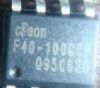
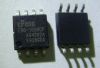
DescriptionThe EN25F16 is a 16M-bit (2048K-byte) Serial Flash memory, with advanced write protection mechanisms, accessed by a high speed SPI-compatible bus. The memory can be programmed 1 to 256 bytes at a time, using the Page Program instruction.The EN25F16 is designed to allow either single Sector at a time or full chip erase operation. The EN25F16 can be configured to protect part of the memory as the software protected mode. The device can sustain a minimum of 100K program/erase cycles on each sector.
Features of the EN25F16 are:(1)lockable 512 byte OTP security sector; (2)minimum 100K endurance cycle; (3)industrial temperature range; (4)write protect all or portion of memory via software; (5)enable/disable protection with WP# pin.The SPI Serial Data Input (DI) pin provides a means for instructions, addresses and data to be serially written to (shifted into) the device. Data is latched on the rising edge of the Serial Clock (CLK) input pin.
The absolute maximum ratings of the EN25F16 can be summarized as:(1)storage temperature:-65 to 125;(2)plastic packages:-65 to 125;(3)output short circuit current:200mA;(4)input and output voltage:-0.5 to 4.0 V;(5)Vcc:-0.5 to 4.0V.Stresses above the values so mentioned above may cause permanent damage to the device. These values are for a stress rating only and do not imply that the device should be operated at conditions up to or above these values. Exposure of the device to the maximum rating values for extended periods of time may adversely affect the device reliability.Once the device has entered the Deep Power-down mode, all instructions are ignored except the Release from Deep Power-down and Read Device ID (RDI) instruction. Executing this instruction takes the device out of the Deep Power-down mode.Please note that this is not the same as, or even a subset of, the JEDEC 16-bit Electronic Signature that is read by the Read Identifier (RDID) instruction. The old-style Electronic Signature is supported for reasons of backward compatibility, only, and should not be used for new designs. New designs should, instead, make use of the JEDEC 16-bit Electronic Signature, and the Read Identifier (RDID) instruction.

 EN25F16 Data Sheet