Transistor Polarity
: N-Channel
Gate-Source Breakdown Voltage
: +/- 20 V
Mounting Style
: SMD/SMT
Packaging
: Reel
Drain-Source Breakdown Voltage
: 30 V
Maximum Operating Temperature
: + 150 C
Configuration
: Single Quad Drain
Continuous Drain Current
: 5 A
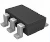
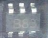
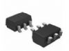
Package / Case
: SSOT-6
Resistance Drain-Source RDS (on)
: 0.035 Ohms
Features: ·5 A, 30 V. RDS(ON) = 0.035 W @ VGS = 10 V RDS(ON) = 0.055 W @ VGS = 4.5 V.
·Proprietary SuperSOTTM-6 package design using copper lead frame for superior thermal and electrical capabilities.
·High density cell design for extremely low RDS(ON).
·Exceptional on-resistance and maximum DC current capability.Pinout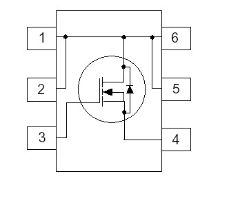 Specifications
|
Symbol |
Parameter |
Ratings |
Units |
|
VDSS
VGSS |
Drain-Source Voltage
Gate-Source Voltage |
30
±20
5
15
1.6
0.8
-55 to 150 |
V
V
A
W
°C |
|
ID |
Drain Current Continuous
Pulsed |
(Note 1a) |
|
PD |
Power Dissipation for Single Operation |
(Note 1a)
(Note 1b) |
| TJ,TSTG |
Operating and Storage Junction Temperature Range |
THERMAL CHARACTERISTICS
RJA
RJC |
Thermal Resistance, Junction-to-Ambient
Thermal Resistance, Junction-to-Case |
(Note 1a)
(Note 1) |
78
30 |
°C/W
°C/W |
DescriptionThis FDC653N N-Channel enhancement mode power field effect transistors is produced using Fairchild's proprietary, high cell density, DMOS technology. This very high density process is tailored to minimize on-state resistance. These devices FDC653N are particularly suited for low voltage applications in notebook computers, portable phones, PCMICA cards, and other battery powered circuits where fast switching, and low in-line power loss are needed in a very small outline surface mount package.
Parameters: | Technical/Catalog Information | FDC653N |
| Vendor | Fairchild Semiconductor |
| Category | Discrete Semiconductor Products |
| Mounting Type | Surface Mount |
| FET Polarity | N-Channel |
| Drain to Source Voltage (Vdss) | 30V |
| Current - Continuous Drain (Id) @ 25° C | 5A |
| Rds On (Max) @ Id, Vgs | 35 mOhm @ 5A, 10V |
| Input Capacitance (Ciss) @ Vds | 350pF @ 15V |
| Power - Max | 800mW |
| Packaging | Tape & Reel (TR) |
| Gate Charge (Qg) @ Vgs | 17nC @ 10V |
| Package / Case | SSOT-6 |
| FET Feature | Logic Level Gate |
| Drawing Number | * |
| Lead Free Status | Lead Free |
| RoHS Status | RoHS Compliant |
| Other Names | FDC653N
FDC653N
FDC653NTR ND
FDC653NTRND
FDC653NTR
|

 FDC653N Data Sheet