Mounting Style
: SMD/SMT
Packaging
: Reel
Maximum Operating Temperature
: + 150 C
Configuration
: Dual
Gate-Source Breakdown Voltage
: +/- 8 V
Transistor Polarity
: N and P-Channel
Package / Case
: SC-70-6
Resistance Drain-Source RDS (on)
: 0.45 Ohms
Drain-Source Breakdown Voltage
: +/- 25 V
Continuous Drain Current
: + 0.5 A, - 0.41 A
Features: ·N-Ch 0.50 A, 25 V, RDS(ON) = 0.45 W @ VGS= 4.5V. RDS(ON) = 0.60 W @ VGS= 2.7 V.
·P-Ch -0.41 A, -25 V,RDS(ON) = 1.1 W @ VGS= -4.5V. RDS(ON) = 1.5 W @ VGS= -2.7V.
·Very small package outline SC70-6.
·Very low level gate drive requirements allowing direct operation in 3 V circuits(VGS(th) < 1.5 V).
·Gate-Source Zener for ESD ruggedness (>6kV Human Body Model).Pinout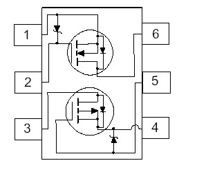 Specifications
|
Symbol |
Parameter |
N-Channel |
P-Channel |
Units |
|
VDSS
VGSS |
Drain-Source Voltage
Gate-Source Voltage |
25
8
0.5
1.5 |
-25
-8
-0.41
-1.2 |
V
V
A
W
°C
kV
|
|
ID |
Drain Current - Continuous - Pulsed |
|
PD |
Power Dissipation for Single Operation |
(Note 1) |
0.3
-55 to 150
6 |
TJ,TSTG
ESD |
Operating and Storage Temperature Ranger
Electrostatic Discharge Rating MIL-STD-883D
Human Body Model (100pf / 1500 Ohm) |
DescriptionThese dual N & P-Channel logic level enhancement mode field effect transistors are produced using Fairchild's proprietary, high cell density, DMOS technology. This very high density process is especially tailored to minimize on-state resistance. This device has been designed especially for low voltage applications as a replacement for bipolar digital transistors and small signal MOSFETS. Since bias resistors are not required, this dual digital FET can replace several different digital transistors, with different bias resistor values.
Parameters: | Technical/Catalog Information | FDG6321C |
| Vendor | Fairchild Semiconductor (VA) |
| Category | Discrete Semiconductor Products |
| Mounting Type | Surface Mount |
| FET Polarity | N and P-Channel |
| Drain to Source Voltage (Vdss) | 25V |
| Current - Continuous Drain (Id) @ 25° C | 500mA, 410mA |
| Rds On (Max) @ Id, Vgs | 450 mOhm @ 500mA, 4.5V |
| Input Capacitance (Ciss) @ Vds | 50pF @ 10V |
| Power - Max | 300mW |
| Packaging | Cut Tape (CT) |
| Gate Charge (Qg) @ Vgs | 1.5nC @ 4.5V |
| Package / Case | SC-70-6 |
| FET Feature | * |
| Lead Free Status | Lead Free |
| RoHS Status | RoHS Compliant |
| Other Names | FDG6321C
FDG6321C
FDG6321CCT ND
FDG6321CCTND
FDG6321CCT
|

 FDG6321C Data Sheet