GS881Z18

Features: • User-configurable Pipeline and Flow Through mode• NBT (No Bus Turn Around) functionality allows zero wait read-write-read bus utilization• Fully pin-compatible with both pipelined and flow through NtRAM™, NoBL™ and ZBT™ SRAMs• IEEE 1149.1 JTAG-...

product image

GS881Z18 Picture
SeekIC No. : 004356231 Detail

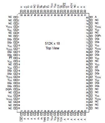
GS881Z18: Features: • User-configurable Pipeline and Flow Through mode• NBT (No Bus Turn Around) functionality allows zero wait read-write-read bus utilization• Fully pin-compatible with bot...

floor Price/Ceiling Price

Part Number:
GS881Z18
Supply Ability:
5000

Price Break

  • Qty
  • 1~5000
  • Unit Price
  • Negotiable
  • Processing time
  • 15 Days
Total Cost: $ 0.00

SeekIC Buyer Protection PLUS - newly updated for 2013!

  • Escrow Protection.
  • Guaranteed refunds.
  • Secure payments.
  • Learn more >>

Month Sales

268 Transactions

Rating

evaluate  (4.8 stars)

Upload time: 2024/4/28

Payment Methods

All payment methods are secure and covered by SeekIC Buyer Protection PLUS.

Notice: When you place an order, your payment is made to SeekIC and not to your seller. SeekIC only pays the seller after confirming you have received your order. We will also never share your payment details with your seller.
Product Details

Description


Features:

• User-configurable Pipeline and Flow Through mode
• NBT (No Bus Turn Around) functionality allows zero wait read-write-read bus utilization
• Fully pin-compatible with both pipelined and flow through NtRAM™, NoBL™ and ZBT™ SRAMs
• IEEE 1149.1 JTAG-compatible Boundary Scan
• On-chip write parity checking; even or odd selectable
• 2.5 V or 3.3 V +10%/10% core power supply
• 2.5 V or 3.3 V I/O supply
• LBO pin for Linear or Interleave Burst mode
• Pin-compatible with 2M, 4M, and 8M devices
• Byte write operation (9-bit Bytes)
• 3 chip enable signals for easy depth expansion
• ZZ pin for automatic power-down
• JEDEC-standard 100-lead TQFP package


Pinout

  Connection Diagram


Specifications

SYMBOL
PARAMETER
Value
UNIT
VDD
Voltage on VDD Pins
0.5 to 2.9
V
VDDQ
Voltage in VDDQ Pins
0.5 to VDD
V
VI/O
Voltage on I/O Pins
0.5 to VDDQ +0.5 ( 4.6 V max.)
V
VIN
Voltage on Other Input Pins
0.5 to VDDQ +0.5 ( 4.6 V max.)
V
IIN
Input Current on Any Pin
+/100
mA
Iout
Output Current on Any I/O Pin
+/-100
mA
PD
Package Power Dissipation
1.5
W
TSTG
storage temperature
-55 to 125
TBIAS
Temperature Under Bias
-55 to 125


Permanent damage to the device may occur if the Absolute Maximum Ratings are exceeded. Operation should be restricted to Recommended Operating Conditions. Exposure to conditions exceeding the Absolute Maximum Ratings, for an extended period of time, may affect reliability of this component.


Description

The GS881Z18/36AT is a 9Mbit Synchronous Static SRAM. GSI's NBT SRAMs, like ZBT, NtRAM, NoBL or other pipelined read/double late write or flow through read/single late write SRAMs, allow utilization of all available bus bandwidth by eliminating the need to insert deselect cycles when the GS881Z18/36AT is switched from read to write cycles.

Because GS881Z18/36AT is a synchronous device, address, data inputs, and read/ write control inputs are captured on the rising edge of the input clock. Burst order control (LBO) must be tied to a power rail for proper operation. Asynchronous inputs of GS881Z18/36AT include the Sleep mode enable, ZZ and Output Enable. Output Enable can be used to override the synchronous control of the output drivers a nd turn the RAM's output drivers off at any time. Write cycles are internally self-timed and initiated by the rising edge of the clock input. GS881Z18/36AT feature eliminates complex offchip write pulse generation required by asynchronous SRAMs and simplifies input signal timing.

The GS881Z18/36AT may be configured by the user to operate in Pipeline or Flow Through mode. Operating as a pipelined synchronous device, in addition to the rising-edgetriggered registers that capture input signals, the GS881Z18/36AT incorporates a rising-edge-triggered output register. For read cycles, pipelined SRAM output data is temporarily stored by the edge triggered output register during the access cycle and then released to the output drivers at the next rising edge of clock.

The GS881Z18/36AT is implemented with GSI's high performance CMOS technology and is available in a JEDECstandard 100-pin TQFP package.


Customers Who Bought This Item Also Bought

Margin,quality,low-cost products with low minimum orders. Secure your online payments with SeekIC Buyer Protection.
Power Supplies - Board Mount
Static Control, ESD, Clean Room Products
Discrete Semiconductor Products
Sensors, Transducers
Undefined Category
Motors, Solenoids, Driver Boards/Modules
View more