Features: ` Meets "PC SDRAM registered DIMM design support document, Rev. 1.2"
` Phase-lock loop clock distribution for synchronous DRAM applications
` External feedback (FBIN) pin is used to synchronize the outputs to the clock input
` No external RC network required
` Support spread spectrum clock (SSC) synthesizersPinout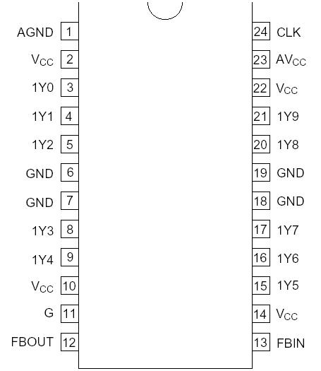 Specifications
| Item |
Symbol |
Ratings |
Unit |
Conditions |
| Supply voltage range |
VCC |
-0.5 to 4.6 |
V |
|
| Input voltage range *1 |
VI |
-0.5 to 4.6 |
V |
|
| Output voltage range *1, 2 |
VO |
-0.5 to VCC+0.5 |
V |
Output : H or L |
| -0.5 to 4.6 |
V |
VCC : OFF |
| Input clamp current |
IIK |
-50 |
mA |
VI < 0 |
| Output clamp current |
IOK |
±50 |
mA |
VO < 0 or VO > VCC |
| Continuous output current |
IO |
±50 |
mA |
VO = 0 to VCC |
Continuous current through
VCC or GND |
ICC or IGND |
±100 |
mA |
|
Maximum power dissipation
at Ta = 25°C (in still air) *3 |
PT |
0.7 |
mW |
|
| Storage temperature |
Tstg |
-65 to 150 |
°C |
|
DescriptionThe HD74CDC2510B is a high-performance, low-skew, low-jitter, phase-lock loop clock driver. It uses a phase-lock loop (PLL) to precisely align, in both frequency and phase, the feedback (FBOUT) output to the clock (CLK) input signal. It is specifically designed for use with synchronous DRAMs. The HD74CDC2510B operates at 3.3 V VCC and is designed to drive up to five clock loads per output.
Bank of outputs provide ten low-skew, low-jitter copies of the input clock. Output signal duty cycles are adjusted to 50 percent independent of the duty cycle at the input clock. Bank of outputs can be enabled or disabled via the control (G) inputs. When the G inputs are high, the outputs switch in phase and frequency with CLK; when the G inputs are low, the outputs are disabled to the logic-low state.
Unlike many products containing PLLs, the HD74CDC2510B does not require external RC networks. The loop filter for the PLL is included on-chip, minimizing component count, board space, and cost.
Because it is based on PLL circuitry, HD74CDC2510B requires a stabilization time to achieve phase lock of the feedback signal to the reference signal. This stabilization time is required, following power up and application of a fixed-frequency, fixed-phase signal at CLK, as well as following any changes to the PLL reference or feedback signals. The PLL can be bypassed for test purposes by strapping AVCC to ground.

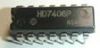
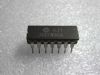
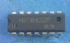
 HD74CDC2510B Data Sheet